Notes of SY EJ, Principles Of Elect. Comm & CEL Ch. 3 Transmitters & Receivers Notes.pdf - Study Material
Page 1 :
ivers, Transmitters and Recelv', , , , <i I>, , tu, , , , , , Syllabus, g with waveforms; Demodulation of AM, , Generation of AM; Block diagram of AM super heterodyne receiver and its workin: es; Concept of pre-emphasis and, signal : Diode detector and practical diode detector; Automatic gain control and its typ ni indirect method (Armstrong, De-emphasis; Generation of FM using direct (varactor diode and reactance modulator) a!, , FM demodulator., method); Block diagram of FM receiver and its working with waveforms; FM detector and PPL as, , , , , , , , Generally, these signals are the harmonics of the, , 3.1 Introduction :, operating carrier frequency and hence to avoid, , - A transmitter is a device, which converts a message a, “ = interference with other transmissions, these unwanted, signal into a signal, which is compatible to the format ., signal frequencies should be filtered out., needed by an antenna system., , - It should produce a carrier signal, which is different 4. Power output, , from all the other signals generated by local oscillators. All the transmitters must provide sufficient power, — It should modulate the carrier using modulating signal output so that the transmitted signal travels longer, before transmission. distance., , — It should provide enough power to the modulated signal | 5, Efficiency, , so that it may travel longer distance. :, Efficiency of the transmitter becomes important, , @ Transmitter requirements i, req because it depends on two important factors :, , 1. Frequency accuracy and stability a) Energy conservation, — The accuracy and stability of transmitter depends’ on b) Heat dissipation j, ssipation in transmission i, the carrier oscillator. a, The overall efficienc, y of an: or z, - The carrier frequency is generally allocated by the power output to the : Seneiities ubiasa, governing body like FCC (Federal Communication’s transmitter contribute oie eee ae, Commission) for any telecommunication system. transmitter, SS eccl efficiency ‘of, 2, Frequency agility 6. Modulation Fidelity, , — It is the ability to change the frequency rapidly without | —, , tuning again and again. basebiana signal; but Capable of Modulating any, i 5 bu ., — This is not the requirement of broadcast transmitter, bandwidth Seni thie Practice, limits on transmitter, 'S this,, 3. Spectral Purity ~ Hence, distortions introduced at the, - Almost all the transmitters produce spuriou: as it is and it becomes imp transmitter remains, ° sible to remove it at the, , , , frequencies.
Page 2 :
a ——— cation (Ms ) 3-2 Transmitters and Receivers, , - This is because the sidebands of AM contains new, frequency components, which are not present in carrier, , , , 3.1.1 AM generation or message signal., , - AM isa linear mod, ig - The modulator has to produce new frequency, — . mu ion technique. This is because components and linear systems never produce new, , ‘on principle is followed in it. frequency components., , - Suppose, ; ‘, , sone a carrier C,(t) is amplitude modulated | - Hence, AM modulators has to be time varying and, Pi ly by two modulating signals m,(t) and m,(t). nonlinear systems., , - It produces modulated Signals e,y)(t) and ean(t) || ~ There are multiple ways to generate AM signal :, Tespectively. 1, Plate modulator 2. Grid modulator, , - Then the effect of modulating the same carrier by the 3. Base modulator 4. Emitter modulator, sum of the two signals, m,(t) and m,(t) ‘or 5. Collector modulator, [m,(t) + m,()], is same as that of the sum of modulated | - The most common amongst is the circuit using BJT, outputs, Collector modulator., , — — That is e4y,(t) + ., anni() + earl) 3.1.2 BUT collector modulator, - But the process involved in generating AM must be, , non Vinear, — The modulator is a linear power device that takes in, , low power modulating signal as input and amplifies it, to obtain high power output., , , , , , - For the basic circuit of BJT collector modulator, refer Fig. 3.1.1 (a)., , , , , , , , , , , , , , , , Voc, Modulating, signal :, O—| om |— SIEn°, . RF bypass capacitor, , Modulating, RF output, , RF drive, , Bias, , , , wenFig. 3,1.1(a) : BJT collector modulator circuit, , i innovation ww SACHIN SHAH Venture, Where Authors, , —
Page 3 :
mitters and Receivers, , , , , , , , , , , , , , Trans!, (1¢2)Fig. 3.1.1 : Output characteristics (b) Collector voltage, (c) Current pulses (d) Modulated output voltage, = Construction @ Working of the modulator, , 1. The transistor is made to operate in class-C amplifier, configuration. Class-C amplifier conducts only for a, portion of the positive half cycle of the input signal., , 2. The carrier signal is fed to the base terminal. This bias, voltage should be sufficient to drive transistor into, conduction region when part of RF is applied,, , 3. The modulating voltage is applied in series with + Ve, through low frequency transformer. It is connected to, the primary of the transformer through power amplifier., , 4. The tuned circuit is connected at the collector. This, tuned circuit is used to resonate the fundamental, frequency component. The modulated output is, extracted from the tuned circuit output., , 5. RF bypass capacitor is connected to provide low, , impedance path., , Tech-Neo Publications .......... Where Authors inspire innovation, ical GAs trees cos sas ws, , , , Case I: When modulating signal is absent., , When the modulating signal is Zero, there will be zero, , modulating voltage across the Secondary of the, transformer., , Therefore, supply Voltage will be directly applied to the, collector and output will be steady sinusoidal RF, carrier only. These are in the form of pulses., , Case II: When modulating signal is present, , Wh a a, , en the modulating Signal is Present, the voltage, acr, , O8s the secondary of the transformer will be added, , to and subtracted from th, ie supph z, collector. PPly voltage given to the
Page 4 :
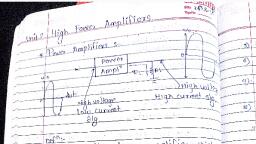
Principles of Electronic Communication (MSBTE,, , _ This varying supply voltage is then applied to the, amplifier. Therefore, the current pulses through, transistor start varying in accordance with the applied, modulating signal., , _ The RF bypass capacitor provides low impedance path, for RF carties signal to ground. Therefore, negligible, RF voltage is produced at the output of secondary of, the transformer., , _ The collector voltage is shown in Fig. 3.1.1(b)., Collector current pulses are shown in Fig. 3.1.1(c)., , _ When the class-C modulator is properly adjusted, the, RF voltage at collector’s output has peak-to-peak value, almost equal to 2V,, as shown. Refer Fig. 3.1.1(d)., , _ The modulated output is obtained through mutual, inductive coupling. The coupling prevents the steady, voltage from being transferred to the output so that the, RF varies about a mean value of zero., , 3.2.1 High Level AM Transmitter, , Refer Fig. 3.2.1., , Microphone, , , , 3.2 AM Transmitters, , Transmitters and Receivers,, , , , wires linear amplification, most of the, , since AM req, modulation in the last, , AM transmitters carry out the, stage of transmission., Based on this, AM transmitters, , 1. High level modulator, , have two types:, , 2. Low level modulator, , High level modulator :, complete in the last stage, it, modulation’. High level modulation is not, with the transmitted power., , Low level modulator : Anything other than this is, Low level modulation, , When the modulation is, , is known as ‘high level, at all related, , known as low level modulation., , is less efficient., , , , , , , , , , , , , , , , , , , , , , , , , , , , , , , , , , , , , , , , , , , , , , , , , , (1ca)Fig. 3.2.1: Block diagram of High level AM transmitter, , > Construction, 1. There are majorly three, (a) Exciter section, , (b) Power section, , different sections in the construction of the high level AM transmi, mitter :, , (c) Modulator section, Where Authors inspire: innovation, aA SACHIN SHAH Venture, , Tech-Neo Publications -—-»-~
Page 5 :
3., , N), 1., , Tech-Neo Publications sasesmues Where Authors, , inciples of Electronic Communication (MSBTE) 3-5, , Exciter section consists of a type of crystal oscillator, circuit and amplifiers. The accuracy of the oscillator is, prime important factor in transmitter,, Buffer amplifier used has high input impedance and, Jow output impedance., Tuned RF amplifiers can have narrow bandwidth or, frequency multipliers like doublers or triplers, as per, need of transmission., Final power amplifier used is Class-C power amplifier,, as it gives high efficiency., Audio processing section consists of preamplifiers,, audio mixers, tone controls, compressors and in-line, amplifiers., Working, Exciter section, , Crystal oscillator : The carrier signal is generated in, the exciter section. The oscillator used in this section is, usually sinusoidal oscillator with crystal controlled, circuitry. This section provides the fidelity of the, carrier frequency. The oscillator frequency is set and controlled by LC tank circuit initially and once the, oscillation starts, crystal takes entire control of, frequency stability., , Buffer amplifier : It performs the function of isolating, two stages in any of the electronic systems. It is, generally low gain impedance matching amplifier., Tuned RF amplifier : Generally two or three, amplifiers stages are used in this stage to provide, maximum gain. The amount of gain depends on the, input received by amplifier and the need of next stage,, that is, final power amplifier., , Modulator section, , Audio section : It comprises of various audio, processing devices to form compatible audio message, , signal needed for modulation purpose. Preamplifiers, , , , innovation, , , , 2., , rm), , 3., , Transmitters and Receivers, , and in i level;, d in-li i the adequate signal s, in-line amplifiers ensure °, iat so as to avoid noise from affecting, for, , ality of the signal. They are required since the output, . :, of microphones are in the range of few microvolts to, , millivolts., Modulator : In high level modulators, final stage carry, , out modulation. It makes use of collector modulated, class-C amplifiers., , Power section, It sets the level of transmission power required by, , antenna system., Power amplifier : The power amplifier takes in the, energy from the DC power supply and converts it to the, AC, which is to be radiated. For obtaining high, efficiency, class-C power amplifier is used., , Driver amplifier : Class-C power amplifier conducts, only for less than one half of the signal cycle. When, this amplifier is conducting, heavy base current flows, through it and final output is obtained with very low, impedance. For this reason, a low power amplifier with, low output impedance, called as driver amplifier, is, used to provide signal input to the power amplifier. It, ensures low input impedance of the final stage, , - amplifier during conduction period., , Advantages, , High efficiency, 100% modulation can be achieved,, Disadvantage, , High power of modulating Signal is required., Application, , Broadcast AM transmitters, , 3.2.2 Low level AM Transmitter, , Refer Fig. 3.2.2,, , ~-A SACHIN SHAH Venture
 Learn better on this topic