Page 1 :
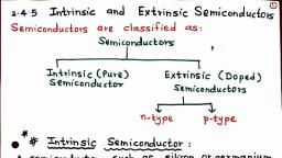
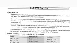
UNIT –II SEMICONDUCTOR PHYSICS, , Engineering physics, , Introduction:At absolute zero a pure, perfect crystal of the most of the semiconductors will be an, insulator. Semiconductors are electronic conductors with electrical resistivity value, generally in the range of, , 102 to 109 ohm-cm at room temperature, intermediate, , between good conductors ( 106 ohm-cm) and insulators ( 1014 to 1022 ohm-cm). The, electrical resistivity of semiconductors dependent on temperature. Devices based on, the properties of semiconductors include transistors, rectifiers, modulators, detectors,, thermostats, and photocells. Broadly speaking we can have two types of, semiconductors i.e. intrinsic semiconductors and extrinsic semiconductors., , INTRINSIC SEMICONDUCTORS:1. A pure semiconductor is called intrinsic semiconductor. At absolute zero, the valence, band of an intrinsic semiconductor is completely filled. For this reason at absolute zero, they behave as insulators., , 2. However, as the temperature is gradually increased some of the electrons of the, valence band get excited to conduction band. The excitation of electrons from the, valence band to the conduction band leaves an equal number of holes in the valence, band., , Vignana Bharathi Institute of Technology, , Page 1
Page 2 :
UNIT –II SEMICONDUCTOR PHYSICS, , Engineering physics, , 3. Both electron in the conduction band and holes in the valence band serve as charge, carriers and contribute to the electrical conductivity. Pure form of the germanium and, silicon are the best examples of intrinsic semiconductors., , EXTRINSIC SEMI-CONDUCTORS: If a small amount of a pentavalent (or) trivalent impurity is introduced into a pure, germanium (or) silicon crystal, the conductivity at the crystal increases appreciably and, the crystal becomes an “Extrinsic” Semi-conductor., Extrinsic semi-conductors are of two types: n- type and p- type., , n- Type semiconductors: 1. When a pentavalent (antimony, phosphorus (or) arsenic) atom replaces a Ge, atom in the crystal lattice. Four of its five valence electrons form covalent bonds, with neighboring Ge (or) Si atoms., 2. The fifth electron free at room temperature to move about in the crystal and acts, as a charge carrier. The crystal is now called an “n- type semi-conductor”, because it has an excess of negative charge carries. The impurity is called a, “donor” because it donates the conducting electrons., 3. In the energy level diagram, the impurity atoms introduce discrete energy levels, for the electrons just below the conduction band. These are called “donor, , Vignana Bharathi Institute of Technology, , Page 2
Page 3 :
UNIT –II SEMICONDUCTOR PHYSICS, , Engineering physics, , impurity levels”., , 4. Therefore, at room temperature, the ‘fifth’ electrons of donor atoms are, thermally excited from the donor levels into conduction band., 5. At ordinary temperature, almost all the electrons in the conduction band come, from the donor levels. Only a few come from the valence band. Therefore, the, main charge carriers responsible for conduction are electrons contributed by the, donors. Thus, in an n-type semi-conductor the electrons are the “majority, carriers” and the holes are “minority carriers”., , Generation and recombination:, When the covalent bond is break it leads to the electron and hole formation. The, electron is in the conduction band and the hole is in the valence band., This electron -hole formation is known as generation., , In the electron-hole formation the number of electrons are generated would be equal to, , Vignana Bharathi Institute of Technology, , Page 3
Page 4 :
UNIT –II SEMICONDUCTOR PHYSICS, , Engineering physics, , the number of holes produced., In the recombination process the electron in the conduction band may lose its energy, and fall into the valence band and it merges with hole. This transfer of the free electron, into the valence band and forms the covalent bond. In this process electron-hole pair, disappears and energy is emitted. Tis process is known as recombination., , Diffusion:, The process by which, charge carriers (electrons and holes) in a semiconductor moves, from a region of higher concentration to a region of lower concentration without any, external voltage is known as diffusion., Or, Without external voltage there is a movement of charges provided a concentration, gradient of charges is exist, this is known as diffusion., The current density due to the diffusion is directly proportional to the concentrate, gradient., , Carrier concentration in Intrinsic Semiconductor:Calculation of density of electrons:Let dn be the number of electrons available between the energy ranges E and E dE in, the conduction band is, dn g ( E ) F ( E )dE ---------------------------- (1), , Where g ( E )dE is the density of electrons in the energy interval E and E dE .we know, that, , 3, 1, 4, 2, g ( E )dE 3 (2m) E 2 dE, h, , Since electron is moving in a periodic potential, its mass has to be replaced by its, effective mass me* and E starts at the bottom of the conduction band Ec , then, 3, 1, 4, * 2, g ( E )dE 3 (2me ) ( E Ec ) 2 dE, h, 1, 2, , c( E Ec ) dE ------------------------------- (2), Vignana Bharathi Institute of Technology, , Page 4
Page 5 :
Engineering physics, , UNIT –II SEMICONDUCTOR PHYSICS, 3, 4, * 2, Where c 3 (2me ), h, , In equation (1) F ( E ) is the probability occupancy of the electrons for a given energy, level E. i.e., , 1, ------------------------- (3), E EF , 1 exp, , KT , , F (E) , , Now from equation (1),(2) and (3), 1, 2, , dn c( E Ec ) F ( E )dE, Now to obtain total number of electrons in the conduction band at any temperature we, have integrate equation (1) from Ec to Etop ., Etop, , , , n, , 1, , c ( E Ec ) 2, , Ec, , 1, E EF, 1 exp , KT, , , , , , dE, , For all possible temperatures E EF KT , so that the term unity in the denominator is, neglected. Then, Etop, , c( E E ), , n, , c, , Ec, , Etop, , , , c(E E ), c, , 1, 2, , Ec, , 1, 2, , 1, E EF, exp , KT, , , , , , dE, , E EF , exp , dE, KT , , , In the above integral the upper limit is taken as infinity. Since the probability of, electrons occupying upper level of conduction band is zero at infinity., , , E EF , n c( E Ec ) exp , dE ---------------------- (4), KT , , Ec, 1, 2, , To solve this integral let us assume that, , E Ec, x, KT, , E Ec kT x, dE kT dx, , Vignana Bharathi Institute of Technology, , Page 5
Page 6 :
Engineering physics, , UNIT –II SEMICONDUCTOR PHYSICS, f E Ec then x 0, and E then x , , Now equation (4) becomes, , , E Ec Ec EF, n c ( E Ec ) exp , KT, , Ec, 1, 2, , , , , dE, , , E Ec , Ec EF , n c ( xKT ) exp , exp, , KT dx ( KT ), KT, , , , , 0, 1, 2, , E EF , n c ( KT ) exp c, KT , , 3, 2, , E EF , n c ( KT ) exp c, KT , , 3, 2, , , , 1, EE , x, 0 2 exp KT c dx, , , , x, , 1, 2, , e x dx --------------------------- (5), , 0, , Simplifying above integral, we get, , , x, , 1, 2, , e x dx , , 0, , , , 1, 2, , 2, , Now equation (5) becomes, 1, 2, , E EF , n c( KT ) exp c, KT 2, , 3, 2, , , , 12, 4, , n 3 (2m ) ( KT ) , 2, h, , , 3, * 2, e, , , e, , , , , 3, 2, , 3, 2, , , , 2 m e * kT , n 2, e, 2, h, , , , Ec EF , , KT , , Ec E F , , KT , , i.e. the number of electrons per unit volume of the material is given by, 3, 2, , , , 2 m e * k T , n 2, e, 2, h, , , Vignana Bharathi Institute of Technology, , Ec E F , , KT, , , ------------------ (6), , Page 6
Page 7 :
UNIT –II SEMICONDUCTOR PHYSICS, , Engineering physics, , Calculation of density of holes:Let dp be the number of holes available between the energy ranges E and E dE in the, valence band is, dp g ( E ) 1 F ( E ) dE ------------------------------ (7), , Where g ( E )dE is the density of holes in the energy interval E and E dE . We know that, g ( E ) dE , , 3, 1, 4, 2, 2, (2, m, ), E, dE, 3, h, , Since hole is moving in a periodic potential, its mass has to be replaced by its effective, mass mh* and Ev is the energy of the top of the valence band, 3, 1, 4, * 2, g ( E )dE 3 (2mh ) ( Ev E ) 2 dE, h, , 1, 2, , c( Ev E ) dE ------------------------------- (8), Where c , , 3, 4, * 2, (2, m, ), h, h3, , In equation (7) 1 F ( E ) is the probability of existence of holes in the valence band., For all possible temperatures EF E KT , so that the term unity in the denominator is, neglected. Then, 1 F (E) , , 1, E E, exp F, 1, KT , , E E, 1 F ( E ) = exp F, , KT , , , Now equation (7) becomes, 1, , dp c( Ev E ) 2 1 F ( E ) dE, , E E, p c ( Ev E ) exp F, dE, KT , , 1, 2, , Now to obtain total number of holes in the valence band at any temperature we have, integrate equation (1) from Ev to ., , Vignana Bharathi Institute of Technology, , Page 7
Page 8 :
Engineering physics, , UNIT –II SEMICONDUCTOR PHYSICS, p, , Ev, , 1, 2, , E EF , E ) exp , dE ------------------------ (9), KT , , c( E, , v, , , , Now equation (9) becomes, E, , 1, v, E E E E, p c(Ev E)2 exp F V V, dE, KT, , , , Ev, , E E EF EV, p c(Ev E) exp V, exp , KT , KT, , , 1, 2, , To solve this integral let us assume that, , , dE, , , Ev E, x, KT, , Ev E kT x, dE kT ( dx), , , 1, EF EV 2 x, p c(kT ) exp , x e dx ----------------------------- (10), KT 0, , 3, 2, , Simplifying above integral, we get, , , x, , 1, 2, , 1, , e x dx , , 2, 2, , 0, , Now equation (10), E EV, p c (kT ) exp F, KT, , 3, 2, , 1, 2, , 2, , , , , , , , , 3, , 2 mh* KT 2, EF EV , p 2, exp , , 2, h, KT , , , , i.e. the number of holes per unit volume of the material is given by, 3, 2, , , , 2 mh KT , p 2, e, h2, , , *, , E F EV , KT , , ---------------------- (11, , Intrinsic carrier concentrations:In an intrinsic semiconductor n p ni is called intrinsic carrier concentration., , Vignana Bharathi Institute of Technology, , Page 8
Page 10 :
Engineering physics, , UNIT –II SEMICONDUCTOR PHYSICS, , e, , 2 EF , KT , , , , e, , EV E c , , , , KT, , , , m , h* , me , *, , 3, 2, , m, , E Ec, 2EF, V, lo g h* , KT, KT, me , *, , m h*, 3, 2 E F K T log *, 2, me, , 3, 2, , , EV E c , , , If we assume that me* mh*, , E Ec , EF v, , 2, , , Thus Fermi level is located half way between the valence band and conduction bands, and its position is independent of temperature., , Carrier concentration in Extrinsic Semiconductor:, Carrier concentration in n- type semi-conductor: Consider an extrinsic semi-conductor doped with donor atoms. The donor atoms, give rise to donor levels Ed close to the conduction band Ec as shown in figure. Let N D, be the number of impurity atoms gives rise to a single electrons state at Ed . Then the, number of electrons in the energy level Ed would be, nd g e Ed Fe Ed ----------------------------------- (1), , But, g e ( Ed ) N D represents the density of states and, 1, , Fe ( ED ) , e, , Ed E F, kT, , --------------------------------------- (2), 1, , Substituting the above values in equation (1) we get, , 1, , nd N D, e, , Ed E F, kT, , 1, , ------------------------------ (3), , Vignana Bharathi Institute of Technology, , Page 10
Page 11 :
Engineering physics, , UNIT –II SEMICONDUCTOR PHYSICS, , Total number of energy states per unit volume at Ed is N D . The total number of filled, energy state per unit volume at Ed is nd . The total number of vacant energy states per, unit volume at Ed is N D N D nd ., From equation (3), , N D N D , , N D, , N D, , ND, E EF , 1 exp d, , KT , , , , 1, N D 1 , 1 exp Ed EF, , , KT, , , , , , , , , , , Ed EF , exp KT , , , ND , 1 exp Ed EF , , , , KT , , ND, ------------------------------ (4), , E, F Ed , exp , 1, KT , , The density of electrons per unit volume in the conduction band is given by, 2 me* KT , ne 2 , , h2, , , , 3/2, , e, , EF Ec, kT, , ---------------------------------- (5), , Where EF, , =, , Energy of the Fermi level, , EC, , =, , Energy corresponding to the bottom of the conduction band., , Density of empty donors (or) number of vacancies per unit volume in the donor, level of energy Ed is, , N, , ND , e, , D, ( E F Ed ), KT, , 1, , ---------------------------------------- (6), , The concentration of electrons in conduction band must be equal to the number, of vacancies per unit volume in the donor level. Therefore, equating equations (5) and, (6), , 2 me* KT , 2, , h2, , , , 3/ 2, , e, , EF Ec, KT, , N, , , e, , D, ( EF Ed ), KT, , -------------------------------- (7), , 1, , Vignana Bharathi Institute of Technology, , Page 11
Page 12 :
Engineering physics, , UNIT –II SEMICONDUCTOR PHYSICS, , If we suppose EF Ed kT . We can neglect 1 from the denominator of R.H.S. of, equation (7). Hence,, , 2 me* KT , 2, , h2, , , , 3/2, , e, , N, , , e, , 2 me* KT , 2, , h2, , , 2 me* KT , 2, , 2, h, , , , EF Ec, KT, , 3/2, , e, , EF Ec, KT, , D, EF Ec, KT, , N, , , e, , 3/2, , e, , EF Ec, KT, , D, EF Ed, KT, , N D .e, , ( Ed E F ), KT, , Taking log on both sides, we get, 2 me* KT EF EC, E EF, log 2 , log N D d, , 2, h, KT, KT, , , , 2 EF Ec Ed, ND, log, 3/ 2, KT, 2 me* KT , 2, , h2, , , ND, 2 EF Ec Ed KT .log, 3/ 2, 2 me* KT , 2, , h2, , , ND, 2 EF Ec Ed KT .log, 3/2, 2 me* KT , 2, , h2, , , , EF , , EC Ed KT, ND, , .log, 3/ 2 ----------------- (8), 2, 2, 2 me* KT , 2, , h2, , , , Putting the value of EF from equation (8) in equation (5), we get, , ND, Ed Ec KT, , , .log, Ec , 3/2, , *, 2, 2, 2 me KT , , , 2, 3/, 2, , 2, *, , , h, 2 me KT , , , ne 2 , , exp , 2, h, kT, , , , , , , , , , , Vignana Bharathi Institute of Technology, , Page 12
Page 13 :
Engineering physics, , UNIT –II SEMICONDUCTOR PHYSICS, , 2 me* KT , 2, , = , h2, , , , 2 me* KT , , h2, , , , 3/ 2, , = 2, , 2 me* KT , ne 2 , , h2, , , , ne 2 N D , , 1/ 2, , 3/2, , , , , , ND, EC , Ed Ec 1, exp , log, , 3/ 2, *, 2 KT, 2, KT , 2 me KT , , , 2, , 2, , , h, , , , , , , , ND, E Ec 1, exp d, log, 3/2, 2 KT, 2, 2 me* KT , , 2, , , , h2, , , , 3/2, , 1/2, , ND , , , 2 , , 1, 2 me* KT , , , h2, , , , 2 me* KT , , , h2, , , , 3/ 4, , e, , , , E, 2 KT, , 3/ 4, , .e, , , , , , , , , , Ed Ec, 2 KT, , ------------------------- (9), , When E Ec Ed ionization energy of the donor., The equation (8) at T = 0 k becomes, EF , , Ed Ec, 2, , This shows that the Fermi level lies exactly halfway between the donor levels and the, bottom of conduction band as shown in figure. But when the temperature is increased, the Fermi level falls below the donor level and at high temperature the value of EF, becomes, , Ec Ev, ., 2, , P- Type semi-conductor: 1. When a trivalent impurity (boron, aluminum, gallium (or) indium) atom replaces a Ge, atom in the crystal lattice. Only three valence electrons are available to form covalent, bands with the neighboring Ge atoms., 2. This results into an empty space (or) a positive hole around the impurity atom. An, electron bound to a neighbouring Ge (or) Si atom drops into the hole, when an external, field is applied, thereby creating a new hole. This phenomenon continues and the hole, moves in the crystal lattice, acting as a positive charge – carrier. The crystal is called a ptype semi-conductor because it has an excess of positive charge carriers. The, Vignana Bharathi Institute of Technology, , Page 13
Page 14 :
UNIT –II SEMICONDUCTOR PHYSICS, , Engineering physics, , impurity is called an ‘acceptor’ because the impurity atoms create holes which accept, electrons., In the energy level diagram the trivalent impurity atoms introduce vacant discrete levels, just above the top of the valence band. There are called “acceptor impurity levels”., , At room temperature, electrons are easily excited from the valence band into the, acceptor levels. The corresponding holes created in the valence band are the main, charge carries in the crystal when an electric field is applied., Thus, in a p- type semi-conductor the holes are the majority carriers and few, electrons, thermally excited from the valence band into conduction band are minority, carriers., Carrier Concentration p-type semi-conductor: Consider a semi-conductor doped with N A number of acceptor atoms per unit, volume. The acceptor atoms give rise to acceptor levels Ea slightly above the valence, band energy Ev as shown in figure., If some of the atoms, let na get ionized by accepting electrons, then those atoms, are becoming negatively charged., The number of such electrons na occupying energy level Ea would be, na g e ( Ea ) Fe ( Ea ) N A ----------------------------------- (1), , But g e ( Ea ) N A represents the density of states and, , Vignana Bharathi Institute of Technology, , Page 14
Page 15 :
Engineering physics, , UNIT –II SEMICONDUCTOR PHYSICS, Fe ( E ) , , na , , 1, E EF , 1 exp a, , KT , , NA, N A ------------------------------------ (2), E, , E, , F , 1 exp a, , KT, , , , Since Ea EF KT , e, , Ea EF, KT, , is a large quantity and thus 1 can be neglected from, , denominator., Number of electrons per unit volume in acceptor level, , N Ae, , EF Ea, kT, , ---------------------------------------------- (3), , Since we have neglected the effect of conduction band, the number of electrons in the, acceptor level is equal to the number of holes in valence band., The density of holes per unit volume in the valence band is given by, , 2 mh* KT , nh 2 , , h2, , , , 3/2, , e, , Ev EF, KT, , ----------------------------------- (4), , Now, equating equation (3) and (4), , 2 mh* KT , 2, , h2, , , , 3/2, , e, , Ev EF, KT, , N A .e, , EF Ea, KT, , ------------------------------- (5), , Taking log of both sides (5) we get, , 2 mh* KT , log 2 , , h2, , , , 3/2, , , , Ev EF, E Ea, log N A F, KT, KT, , 2 mh* KT , Ev EF EF Ea, log N A log 2 , , KT, h2, , , , Vignana Bharathi Institute of Technology, , 3/2, , Page 15
Page 17 :
UNIT –II SEMICONDUCTOR PHYSICS, , Engineering physics, , This represents the carrier concentration in P-type semiconductor., At T = 0k, the form of equation (6) becomes, , EF , , Ea Ev, 2, , Hence, in this case, the Fermi level lies exactly halfway between the acceptor, levels and the top of valence band., But when T increases the Fermi level rises., At high temperature the value of EF becomes, , Ea Ev, i.e., EF approaches the center of, 2, , band gap and crosses the acceptor level which makes the substance an intrinsic semiconductor., It is clear from equation (7) that density of the holes in the valence band is proportional, to the square root of the acceptor concentration., , HALL EFFECT:, When a current carrying material or semiconductor is placed in a transverse magnetic, field then a potential difference is developed across the semiconductor which is, mutually perpendicular to both the electric and magnetic fields. This phenomenon is, known as Hall Effect., The voltage produced in this phenomenon is known as Hall Voltage (VH), , Vignana Bharathi Institute of Technology, , Page 17
Page 18 :
Engineering physics, , UNIT –II SEMICONDUCTOR PHYSICS, , From the Lorentz force FL e E, , --------------- (1), , E ---- is Applied electric field, , e ---- is charge of the electron or hole, The magnetic force acting on the charges is given as, , FB B e vd, , ------------- (2), , B ---- is magnetic field, , vd, , From eq (1) and (2) we get, , is drift velocity, , e EH B e vd, , EH B vd --------- (3), The applied electric field EH is written as, , EH , , VH, d, , ----------- (4), , VH is Hall Voltage and d is thickness of the sample., From the above equations we get, , VH, B vd, d, , VH B vd d ---------- (5), Due to the Hall field there will be development of current density J, , J n e vd, vd , , J, --------- (6), ne, , Therefore VH B, , J, d --------- (7), ne, , But we know the current density J in terms of current is, , J, , I, I, J , ------- (8), A, dw, , Where A d w, , d, , is thickness of the sample and, , w, , is width of the sample., , Substitute the equations (6) and (7) in (5) we get, Vignana Bharathi Institute of Technology, , Page 18
Page 19 :
Engineering physics, , UNIT –II SEMICONDUCTOR PHYSICS, , VH B, , VH , , I 1 , , d, d wn e, , BI 1 , , -------- (9), w n e, , This equation represents the Hall Voltage., , Hall Coefficient (RH):, It can be defined as it is the ration of the electric field across the semiconductor to the, current density per unit volume per unit magnetic field., , i.e., RH , , EH, J B, , V 1, i.e., RH H , d J B, , From equation (4), , Substitute the value of VH from eq (7) in the above equation, , RH B, , J, 1, d, dne J B, , RH , , 1, ne, , This equation represents the Hall coefficient., , Applications of Hall Effect:, Hall Effect is a very useful phenomenon and helps to, , Determine the Type of Semiconductor:, By knowing the direction of the Hall Voltage, one can determine that the given sample is, whether n-type semiconductor or p-type semiconductor. This is because Hall coefficient, is negative for n-type semiconductor while the same is positive in the case of p-type, semiconductor., , if RH ve it is n-type semiconductor and if RH ve it is p-type semiconductor., Vignana Bharathi Institute of Technology, , Page 19
Page 20 :
UNIT –II SEMICONDUCTOR PHYSICS, , Engineering physics, , Calculate the Carrier Concentration:, The expressions for the carrier concentrations of electrons (n) and holes (p) in terms of, Hall coefficient are given by n , , 1, 1, and p , e RH, e RH, , Determine the Mobility (Hall Mobility):, Mobility expression for the electrons (μn) and the holes (μp), expressed in terms of Hall, coefficient is given by,, , n n RH and p p RH, , Where, σn and σp represent the conductivity due to the electrons and the holes,, respectively., , Measure Magnetic Flux Density:, This equation can be readily deduced from the equation of Hall voltage and is given by, , VH , , VH w, BI 1 , , B R I, w n e, H, , Further, there are many commercially available types of equipment based on the, principle of Hall effect including Hall-effect sensors and Hall-effect probes., , Formation a PN junction: A P-N junction is formed by joining P-type and N-type semiconductors to, gather in very close contact. The term junction refers to the boundary, interface where two regions of the semiconductor meet. In N- type the, “donor” ion is represented by plus sign because, after this impurity atom, donates an electron it becomes a positive ion and in P-type acceptor ion is, indicated by minus sign because, after this atom accepts an electron, it, becomes a negative ion., , Vignana Bharathi Institute of Technology, , Page 20
Page 21 :
UNIT –II SEMICONDUCTOR PHYSICS, , Engineering physics, , Space-charge region: There is a large concentration of holes in the P-type material and a large, concentration of electrons in the N-type material. Because there is density, gradient across the junction, holes will initially diffuse to the right across the, junction, and electron to left. The flow of holes from P-region results a, negatively charge acceptor ions and flow of electrons from N-region leaves, positively charged donor ions., The unneutralized ions in the neighborhood of the junction are referred to as, “uncovered charges”. Since the region of the junction is depleted of mobile, charges, it is called depletion region, the space-charge region or transition, region. The thickness of this region is of the order of the wavelength of visible, light ≈ 0.5 micron., , Energy diagram of the PN junction: The valence and conduction bands in an n-type material are at slightly lower, energy levels than the valence and conduction bands in a p-type material., This is due to differences in the atomic characteristics of the penta valent, and the trivalent impurity atoms., , Vignana Bharathi Institute of Technology, , Page 21
Page 22 :
UNIT –II SEMICONDUCTOR PHYSICS, , Engineering physics, , An energy diagram for a p-n junction at the instant of formation is shown in, Figure. As you can see, the valence and conduction bands in the n region are at, lower energy levels than those in the p region, but there is a significant amount of, overlapping., The free electrons in the n region that occupy the upper part of the conduction, band in terms of their energy can easily diffuse across the junction (they do not, have to gain additional energy) and temporarily become free electrons in the lower, part of the p-region conduction band. After crossing the junction, the electrons, quickly lose energy and fall into the holes in the p-region valence band as indicated, in above Figure., As the diffusion continues, the depletion region begins to form and the energy level of, the n- region conduction band decreases. The decrease in the energy level of the, conduction band in the II region is due to the loss of the higher-energy electrons that, have diffused across the junction to the p region. Soon, there are no electrons left in, the n-region conduction band with enough energy to get across the junction to the pregion, conduc, tion, band., , Vignana Bharathi Institute of Technology, , Page 22
Page 23 :
UNIT –II SEMICONDUCTOR PHYSICS, , Engineering physics, , At this point, the junction is at equilibrium; and the depletion region is complete, because diffusion has ceased. There is an energy gradient across the depletion region, which acts as an "energy hill" that an n-region electron must climb to get to the p, region., I-V Characteristics of PN Junction:, The V-I characteristics or voltage-current characteristics of the p-n junction diode is, shown in the graph. X-axis represents the voltage applied across the p-n junction diode, whereas Y-axis represents the current flows in the p-n junction diode., , Forward Bias:, If the positive terminal of the battery is connected to the p-type semiconductor and the, negative terminal of the battery is connected to the n-type semiconductor, the diode is, said to be in forward bias. In forward biased p-n junction diode, VF represents the, forward voltage whereas IF represents the forward current., , Vignana Bharathi Institute of Technology, , Page 23
Page 24 :
UNIT –II SEMICONDUCTOR PHYSICS, , Engineering physics, , When the external voltage applied on the diode, then it starts allowing large electric, current through it. At this point, a small increase in voltage increases the electric current, rapidly., The forward voltage at which the diode starts allowing large electric current is called, cut-in voltage., , Reverse biasing:If the negative terminal of the battery is connected to the p-type semiconductor and the, positive terminal of the battery is connected to the n-type semiconductor, the diode is, said to be in reverse bias., In reverse biased p-n junction diode, VR represents the reverse voltage whereas IR, represents the reverse current., , If the external reverse voltage applied on the p-n junction diode is increased, the free, electrons from the n-type semiconductor and the holes from the p-type semiconductor, are moved away from the p-n junction. This increases the width of depletion region., , Vignana Bharathi Institute of Technology, , Page 24
Page 25 :
UNIT –II SEMICONDUCTOR PHYSICS, , Engineering physics, , Then it does not allow the majority charge carriers but it allows the minority charge, carrier current., , The free electrons (minority carriers) in the p-type semiconductor and the holes, (minority carriers) in the n-type semiconductor carry the electric current. The electric, current, which is carried by the minority charge carriers in the p-n junction diode, is, called reverse current., In n-type and p-type semiconductors, very small number of minority charge carriers is, present. Hence, a small voltage applied on the diode pushes all the minority carriers, towards the junction. Thus, further increase in the external voltage does not increase, the electric current. This electric current is called reverse saturation current., , Direct and Indirect band gap semiconductors:The relationship between kinetic energy Ek and k is given by, Ek , , k 2, ---------------- (1), 2me*, , Where me* is effective mass of the electron., From the above equation Ek vs. k is parabola curving upward in energy for, increasing value of ‘k’. From the fig the parabolic energy band, which is known as, the “conduction band”., Vignana Bharathi Institute of Technology, , Page 25
Page 26 :
UNIT –II SEMICONDUCTOR PHYSICS, , Engineering physics, , The downward curve refers to the band of possible energy levels known as, the “valence band”. Where electrons reside but cannot easily move around. The, negative curve for the valence band can be described by using a negative effective, mass., , There are two basic types of arrangement of the conduction band and valence, band in semiconductor materials, , , Direct band gap semiconductors, , , , Indirect band gap semiconductors, , Direct band gap semiconductors: In direct band gap semiconductors the upper band (conduction band) and, lower band (valence band) have their minimum and maximum at same, value of ‘k’, Electrons near the top of the valence band are able to make transition to, states near the bottom of the conduction. This process is called, “Fundamental absorption”, , Vignana Bharathi Institute of Technology, , Page 26
Page 27 :
UNIT –II SEMICONDUCTOR PHYSICS, , Engineering physics, , Here electron decay from the conduction band can recombine with holes in, the valence band and directly emitting a photon of energy “ h ”, Life time(recombination time) of charge carriers is very less, Due to recombination process these are used in fabrication of LED and, LASER diodes., Indirect band gap semiconductors: Indirect band gap semiconductors in which the bottom of the conduction, band does not lie at the origin., , Vignana Bharathi Institute of Technology, , Page 27
Page 28 :
UNIT –II SEMICONDUCTOR PHYSICS, , Engineering physics, , In indirect band gap semiconductors have displacement in ‘k’ between the, minimum of the upper band and lower band., In this case the electron cannot make a direct transition from the top of the, valence band to the bottom of the conduction band., In these materials also transition takes place, but as a two-step process., The electrons absorbs both a photon and phonon supplies the required, momentum., Here an electron from conduction band recombine with a hole valence, band indirectly. The electrons decay to defect level by emitting phonon, .now electrons in defect level combine with holes in valence band by, emitting photons., Life time of charge carries is high, Due to longer life time these are used to amplify the signals as in case of, diodes and transistors., LED or Light Emitting Diode:, Itis a two-lead semiconductor light source. It is a p–n junction diode, which emits, light when activated. When a suitable voltage is applied in forward bias to it,, electrons are able to recombine with electron holes within the device, releasing, energy in the form of photons., The commercially used LED‘s have a typical voltage drop of 1.5 Volt to 2.5 Volt or, current between 10 to 50 mill amperes. The exact voltage drop depends on the, LED current, colour, tolerance., Construction:, An n-type layer is grown on a substrate and a p-type layer is grown on it by the, process of diffusion. The P-region is made very thin to prevent loss of photons, Vignana Bharathi Institute of Technology, , Page 28
Page 29 :
Engineering physics, , UNIT –II SEMICONDUCTOR PHYSICS, , due to absorption in the layer., , Construction of LED, The metal connections are made at the edges of the p-region in order to allow the, light to escape., A metal film is deposited at the bottom of the substrate for reflecting as much as, possible towards surface of the device and provides electron connection., The device is encapsulated in a clear epoxy resin of suitable refractive index., LED WorkingThe P-N junction emits light when electrical energy is applied to it. This, phenomenon is generally called electroluminescence, which can be defined as, The, , process, , ofemitting, , the, , lightby, , a, , semiconductor, , by, , applying, , anelectricalsource ofenergy is called electroluminescence, When the forward bias P-N junction diode is connected the charge carriers, recombine as the electrons cross from the N-region and recombine with the holes, existing in the P-region., The forward voltage across an LED is significantly greater than the ordinary diode., It is in between 1.2V and 3.2V. The amount of light emitted is directly, proportional to the forward current., Free electrons are in the conduction band, while holes are in the valence band., Thus the energy of the holes will be lesser than the energy of the electrons. Some, portion of the energy must be dissipated in order to recombine the electrons and, Vignana Bharathi Institute of Technology, , Page 29
Page 30 :
UNIT –II SEMICONDUCTOR PHYSICS, , Engineering physics, , the holes. This energy is emitted in the form of heat and light., , Forward biased P-N junction, The electrons dissipate energy in the form of heat for Si & Ge diodes but in GaAsP, and GaP semiconductors, the electrons dissipate energy by emitting photons., V-I characteristics of LED:, The forward bias Voltage-Current (V-I) curve and the output characteristics curve, are shown in the figure., , For some forward voltages the LED passes almost no current at all, at least until, the breakdown voltage is reached. For forward voltage the current rises very, steeply when a certain voltage is reached. The minimum voltage required to rise, Vignana Bharathi Institute of Technology, , Page 30
Page 31 :
UNIT –II SEMICONDUCTOR PHYSICS, , Engineering physics, , the current is known as threshold voltage., If the semiconductor is translucent, the junction becomes the source of, light as it is emitted, thus becoming a Light-Emitting Diode, but when the junction, is reverse biased no light will be produced by the LED and, on the contrary, the, device may also be damaged., Advantages of LEDThere are many advantages of using a LED as:, , , It helps in saving energy., , , , Reduction in costs., , , , Self-Ambience Adjustment., , , , Soothes & energizes the environment & People., , , , Enhances the brand with its gorgeous lighting., , , , Environment Transformation., , Semiconductor Photo detectors:, Photo detectors are the devices that absorb optical energy and convert it to, electric energy. The operation of the photoelectric detectors is based on the, internal photoelectric effect., These are mainly three types., 1. Solar cell, 2. P-I-N Diodes, 3. Avalanche Photo Diodes, When the light incident on the semiconductor, electrons are excited from the, valance band to the conduction band leaving holes in the valance band. The free, electrons and holes generated in the material do not leave the material and so, free charge carrier concentration is increases. This is known as internal photo, electric effect., The frequency of the photons satisfies the condition, Vignana Bharathi Institute of Technology, , , , Eg, h, , ., Page 31
Page 32 :
UNIT –II SEMICONDUCTOR PHYSICS, , Engineering physics, , Solar cell:, A solar cell is basically p-n junction that can generate electrical power, when it is, illuminated. i.e., when sun .light incident on the p-n junction it converts the, optical energy into electric energy., The solar cell is so designed that a large area is exposed to light which enhanced, the voltage generation across the terminals of the p-n diode. It doesn’t require, any biasing voltage., Construction & Function:, , , Solar cell essentially consists of s silicon PN junction diode with anti-, , reflecting glass window on top surface of N material., , , The top layer N material is made extremely thin, so that the incident, , photons may easily reach PN junction and strikes the neutral silicon atoms., , , The bottom layer is made up of P-type material is thick layer. These two P-, , type and N type materials are in contact with metal plates., , , When sunlight hits the top layer of silicon solar cell (N type material) is, , absorbed by the solar cell. This light energy knocks the electrons of neutral silicon, atoms in the PN junction and they get separated from the atoms which causes the, generation of electron and hole pair in the depletion layer., , , , These charges develop the electric field in the depletion layer. Due to this, Vignana Bharathi Institute of Technology, , Page 32
Page 33 :
UNIT –II SEMICONDUCTOR PHYSICS, , Engineering physics, , electric field, charges s experiences the electric force ( F Eq )., , , Then a large number of free electrons and holes are generated at the N-, , type and P-type semiconductor when the sunlight incident on it., , , Semiconductor cannot conduct these electrons and holes. Hence a, , conducting wire is connected to the two silicon layers (p-type and n-type layers)., , , An electrical path is created for the free electrons to flow from n-side to p-, , side through the conducting via a load resistor or an electric bulb., , , Due to the charge accumulation on both P and N region a potential, , difference is created which is known as photo voltage., , , The voltage produced from this solar cell is in between 0.5V to 0.6V., , , , The light energy required to create the free electrons should be greater, , than the energy band gap (Eg), V-I characteristics of Solar cell:, V-I characteristics of a solar cell is basically a graphical representation of the, operation of the solar cell., It gives the relation between the current produced and Voltage developed in solar, cell and represents the power delivered by the solar cell is the product of the, current produced and voltage developed (V X I)., , The values of current produced and voltage developed are below the values of Isc, and Voc., Vignana Bharathi Institute of Technology, , Page 33
Page 34 :
UNIT –II SEMICONDUCTOR PHYSICS, , Engineering physics, , Where Isc is maximum current in short circuit at voltage is become zeroand Voc is, maximum voltage in open circuit at which the current become zero., When the solar cell open-circuited, i.e., it is not connected to any load, the, current will be at its minimum (zero) and the voltage across the cell is at its, maximum, known as the solar cells open circuit voltage, or Voc., At the other extreme, when the solar cell is short circuited, that is the positive, and negative leads connected together, the voltage across the cell is at its, minimum (zero) but the current flowing out of the cell reaches its maximum,, known as the solar cells short circuit current, or Isc., The maximum voltage available from a cell is at open circuit, and the maximum, current at short circuit. Of course, neither of these two conditions generates any, electrical power, but there must be a point somewhere in between were the solar, cell generates maximum power., However, there is one particular combination of current and voltage for which the, power reaches its maximum value, at Im and Vm., In other words, the point at which the cell generates maximum electrical power, and this is shown in the graph as rectangle. This is the “maximum power point”, or MPP., Fill Factor of Solar Cell:, The ratio between product of current and voltage at maximum power point to the, product of short circuit current and open circuit voltage of the solar cell., It gives the efficiency of the solar cell., , Vignana Bharathi Institute of Technology, , Page 34
Page 35 :
UNIT –II SEMICONDUCTOR PHYSICS, , Engineering physics, , P-I-N Diode:, A PIN photodiode is made of P region and N region separated by a highly resistive, intrinsic layer. The intrinsic layer is placed between the P region and N region to, increase the width of depletion region., The P-type and N-type semiconductors are heavily doped. Therefore, the P region, and P region of the PIN photodiode has large number of charge carriers to carry, electric current., On the other hand, intrinsic semiconductor is an undoped semiconductor, material. Therefore, the intrinsic region does not have charge carriers to conduct, electric current., Under reverse bias condition, the majority charge carriers in N region and P, region moves away from the junction. As a result, the width of depletion region, becomes very wide. Therefore, majority carriers will not carry electric current, under reverse bias condition., However, the minority carriers will carry electric current because they experience, repulsive force from the external electric field., In PIN photodiode, the charge carriers generated in the depletion region carry, most of the electric current. The charge carriers generated in the P region or N, region carry only a small electric current., When light or photon energy is applied to the PIN diode, most part of the energy, is observed by the intrinsic or depletion region because of the wide depletion, width. As a result, a large number of electron-hole pairs are generated., Free electrons generated in the intrinsic region move towards N-side whereas, holes generated in the intrinsic region move towards P-side. The free electrons, and holes moved from one region to another region carry electric current., , Vignana Bharathi Institute of Technology, , Page 35
Page 36 :
UNIT –II SEMICONDUCTOR PHYSICS, , Engineering physics, , When free electrons and holes reach N region and P region, they are attracted, towards the positive and negative terminals of the battery., The population of minority carriers in PIN photodiode is very large compared to, the PN junction photodiode. Therefore, PIN photodiode carry large minority, carrier current than PN junction photodiode., When forward bias voltage is applied to the PIN photodiode, it behaves like a, resistor., , Avalanche photodiode:, The operation of avalanche photodiode is similar to the PN junction and, PIN photodiode. The main deference is that a high reverse bias voltage is, applied in case of avalanche photodiode to achieve avalanche, multiplication., The generation of free carriers that are created by absorbed photons is, known as avalanche multiplication, Applying high reverse bias voltage to the avalanche photodiode will not, , directly increase the generation of charge carriers. However, it provides, Vignana Bharathi Institute of Technology, , Page 36
Page 37 :
UNIT –II SEMICONDUCTOR PHYSICS, , Engineering physics, , energy to the electron-hole pairs generated by the incident light., When light energy is applied to the avalanche photodiode, electron-hole, pairs are generated in the intrinsic region. This causes the high electric field, at the junction region., It is extremely high electric field region is created is approximately equal to, about 3X10⁵ V/cm., Due to the reverse voltage the electron-hole pairs experience an electric force, and move towards junction at high speed and collide with the atoms, they knock, off the free electrons., , The newly generated electrons are again accelerated and collides with, other atoms, a large number of minority carriers are generated., Thus avalanche photodiodes generate more number of charge carriers than, , PN and PIN photodiodes., Avalanche photodiodes are used in the applications where high gain is an, , important factor., , Vignana Bharathi Institute of Technology, , Page 37