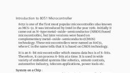
Page 1 :
2., , Computer System, , 2-11, , DigitalSys.&Architecture (MU-B.Sc.Comp.), Polling, , Disadvantages, Master 2, , Master 1, , Master n, , Polling requires, , 1., , masters to, , of, , count, Poll, , ontroler, , number, control lines. Maximum, , be connected, , lines. With, , poll, , n, , to, , bus is restricted, , count, , lines,, , by poll, have, , can, , we, , maximum of 2 masters., , count, Hnes, , Bus, , more, , 2., Bus request, , Delay, , could become, in granting control of bus, devices to be polled is large., , large if, , the number of, , Bus, busy, Data transier, , 3., , bus, , Fig. 2.7.2:, , Independent requesting, Master 2, , Mastor 1, , using polling, , Bus arbitration, , Master n, , Bus Grant1, each, Polling is process of calling, , by, , master is called, , its address. Address of, , generated on poll count, Poll, , lines, , count, , master turn, , are, , Bus Request 1, , by turn. A, master, , a, , ue Grant 2, Bue, oonirollerL Bus Request 2, , is, , Bus Granln, , lines., , connected to each device. Bus, , line has the, request and Bus busy, , same, , meaning, , as, , in, , the context of daisy chaining., A request, , to, , the bus is made, , use, , line. Bus request will, , not, , on, , the Bus request, , the Bus, be responded to till, , line, , controller, , lines. Each, , to a, , responds, , master, , (device, , signal, , on, , in sequence, , addresses, , by generating, , Fig. 2.7.3:, , Bus arbltration, , - I n this, , scheme, each, , or, , Bus request, , on, , poll, , count, , processor) is assigned, , a, , The arbitration among, , count, , matches,, , of, the address, , In, , arbiter., , central, , requesting, , has its independent Bus, , masters, , case, , master can, , quickly., , is still carried out, , on, , a, , requests,a, , of multiple, , be selected, , by, , the basis of, , priority., , Normally,, , poll, , master, , the, line. In this scheme, request and Bus grant, immediate, master is almost, identification of requesting, , unique address., When the, , using independent requesting, , and the request can be responded, , busy line is active., The bus, , bus, , a, , the, for the bus,, that is requesting, starts using, signal and, the Bus busy, , we, , transactions, , use, , and, , priority-based, , policy for 1/0, , policy, , fairness-based, , among the, , processors., , particular master, master activates, , the bus., , Input/OutputSystem, There, , are a, , wide, , variety of peripherals, , different, that deliver, , Advantages, Priority can be, the generation, , Failure, , 2.8, , of one, , changed, , by, , of a d d r e s s e s, master, , (a, , affect any other master., , changing, , on, , the poll, , device or, , the, , sequence, , count, , of, , lines., , processor), , will not, , amounts, , or, , of data, , 1/0, , devices, , at different, , formats. All these devices are, and in different, interface these, and RAM and hence to, slower than CPU, modules., a need of 1/0, to the CPU there is, , speeds, , devices, , Input/Output, with, , and, Module is interface to CPU, , one or more, , Memory, , peripherals., , Pubiicatioms
Page 2 :
Computer System, , Digital Sys. &Architecture (MU-B.Sc. Comp.), The, , 2-12, , general, , model of 1/0 Module interfacing with, system bus is shown in Fig. 2.8.1., , We will consider, , only digital, , microprocessor is, , digital, , data transfer, , Suppose you, , circuit., , B. There, Point A to Point, transfer data from, , Address ines, , possible ways, , System, , Data lines, , bus, , want, are, , to, , two, , of doing it:, , Parallel data transfer, , 1., , Control lines, , because, , 2. Serial data transfe., , VO Module, , For, , can, parallel data transfer, we, , are, , connected,, , one, , use, , 8255. Two, , 8255's, , at each side., , The Port A of 8255, 1., , at point A is connected to Port A of 8255, , 2., , at point B. So the data transferred is of 8 bits at a, , Links to, , peripheral, devices, , time. For implementing this communication, we, , Fig. 2.8.1:General model of VO module Interface, , want 8 lines of PA interconnected and line will be, , The various functions of the, 1/0 Module involve, , the common ground between two points., , 1., , Issue of control and, , :, , In serial data transfer the data is transferred serially on, , timing signals, , 2, , Communication with CPU, , a,single line, the same hardware used for parallel data, , 3., , Communication with peripheral, , can, , 8255, , and, , Detection of errors, , The internal block, , diagram, , of 1/0 module is shown in, , Irterace to, , To, , implement, , above communication we, require, line of Port A interconnected and, second line, , Edemal, device, intertaoe, , StatusControl rogisters, , ogic, , Exemal, , logic, , device, inlerface, , Parallel, , vs., , Data, , The data may be a, , Serial Intertace, , The data transfer is, , comparatively faster., 3, , data transfer, , Parallel lines of 8/16/32, bits. Hence, 8/16/32 bits, , Only 1 bit is transmitted, at a time., , simultaneously., , an VO module, , digital or analog in nature., , Serial, , can be transmitted, , Status, , 2., , communication specifies,, , between two points., , methods of data, , Control, , Control, , Fig. 2.8.2:Internal block diagram of, , 2, , Parallel, , Satus, , logic, , nes, , specified, , Data, , 1., , Control, , ground between two points., , Now let's compare the, transfer., , Deta registers, , The word,, , 2., , axdemal device, , Addrees, nes, , 2.8.1, , To Port A of 8255, , i.e. common, , Intertaoe to, , A, , 1., , one, , Fig. 2.8.2., 8ysem Dus, , implement this., , Instead of, connecting all 8 lines connect single line from Pore A of, , Buffering of data between the CPU and peripheral, 5., , also be used to, , Due to, , so, , many, , parallel, paths 'crosstalk among, different bits is, , The data, , transfer is, , comparatively slowe., No'crosstalk' possible., , possible., , This cannot be used, for, , distant communication., , This can be used for, distant communiction
Page 3 :
Digital Sys.&Architecture (MU-B.Sc. Comp.), Parallel, , 2-13, , Serial, , Sr, , Computer System, , 1., , Simplex, , No., , The simplex is one way transmission., , More parallel haro, rdware is, , Less, , required., , required., , it is comparatively, , It is comparatively, , parallel hardware, , such that data transfer takes, , The connection exists, , place only in one direction., data transfer in the other, , There is no possibility, , cheaper, , costlier., , direction., , In these two methods the cost of connecting two distant, , System A is transmitter and system B is receiver only, , noints, is the main factor. So though the parallel data, transfer is faster, it is preferred for small distances, , only. But for long distances, serial data transfer is, , 2., , Duplex, It is further, , two way transmissions., , duplex is, , The, , dividedin 2 groups:, , preferred., , In serial data transfer the 8 bits of data is converted, , into serial 8 bits; using shift register (parallel in serial, , (a) Half duplex, It is, , a connection, , between two terminals such, , that, data, , out mode). These serial bits are transferred on single, , but transmission, may travel in both the directions,, , line using serial 1/0 data transfer. To transfer 8 bits of, , activated in one direction at a time., , data, it will require 8 clock pulses. On the other side, , around after, This indicates that the line has to turn, , exactly opposite process, accepted, , is done. These serial 8 bits, , parallel form, , and converted to, , data. This process is shown in, Parallel, 8 bit data, , senal, , (b) Full duplex, , Serial, o, , Seral, 1 bit data, , paralel, converter, , converter, , Parallel, , It is, , Clock, , a, , connection between two terminals such, , directions, may travel in both the, , 8 bit data, , will, , Clock, , contain, , one, , way, , that, data, , simultaneously. So it, or, , transmission, , two, , way, , transmission at a time., , ulses, , puises, , System, , System, , GND, , GND, , VO Modules and 8089 1O Processor, , 2.9, Serial Vo, , Fig. 2.8.3, 2.8.2, , communication is complete in one direction., , get 8 bits of, , Fig. 2.8.3., , Parallel, to, , to, , are, , Types of Communication Systems, , The communication, , systems, , are, , classified, , on, , the basis, , An, , Input / Output device, , directly to the, using, , an, , I/0, , processor. It, , module., , 1/0, , can, , never, , always has, module is, , to be interfaced, , required for the, , following reasons, , oftransmission:, Types of communication, , 1., , systems, , 1/0, , devices, , are, , slower, , normally, , have different, processor and also, , Hence, (a) Half duplex, , 1/0, , module works as, , processor and, , (b) Full duplex, Types, , speeds., , the, , Hence if, , no, , 2. Duplex, , systems, of communication, , than, , 1/0 module, the processor will have, devices., wait for long time for the 1/0, , there is, , 1. Simplex, , Fig.2.8.4, , be connected, , 1/0, , a, , to, , bufer between the, , device to hold the data for the, , required time, , 2., , Each, , 1/0, , device has different data bus width., , 1/0, , conversion., module does the required width, , ecPUblications, Knemiedge
Page 4 :
2-14, , Digital Sys. &Architecture (MU-B.Sc. ComP, 3., , Each, , Tollowed., , Some, , use, , serlal, , Types, to, , protoco, , 1/0 device has different, , Data, , 2.10, , e, , of, , Programmed, , 1/0 module, , protocol required, , communicates, , by the 1/0, , according, , nterrupt dri, driven, , Interrupt, , VO,, , VO a n d DMA, some, , communication,, , of, , method, , use parallel, some have handshaking signals etc, Hence, , ansfer Techni, Techniques, , Transter, , another, , to the, , yet, , is, , There, , based on, , classifying the, , clases, , how, , devices, , interfacing, , devices., , of 1/0, between, , and when, , and, , essor and, , processor, , the, , transferred, , data is, , 2.9.1, , VO Module, , devices., , this, , under, , 1., , of input, , Need, , module: Each output device, , operates, , at a, , the speed of the processor. Hence,, , an, , are, , There, , different, different speed, has different data format and, than, protocol. Also, most of the 1/0 devices are slower, , driven, , 1/0 and, , programmed, , namely, DMA, , a, , module, , wherein, , mechanism,, , each and every, , mupt, , the processor, , a service, device for it needs, , or, , cherh, necks, , not., , device, , 2.10.1, , In the, , Block dlagram of VO module, , Programmed VO, , programmed 1/0 method, , interfacing,, , of, , CPU has, , direct control over 1/0o., The processor checks the status of the devices and, , Data, bus, , Data register, , issues read or write commands and then transfers data, During the data transfer, CPU waits for 1/0 module to, , Addr, , Addr Addr register, , bus, , complete operation and hence this system wastes the, CPU time., , RD, , WR, , CS, , The sequence of, , Mode and, , operations to, programmed 1/0 operation are:, , control, unit, , Fig. 2.9.2 : Block dlagram of VO module, Data register is used to store the, data given by the, input device to be forwarded to the, processor OR given, by the processor to be forwarded to an, output device., is used to, , device to be accessed., , provide address, , be carried out in, , 1., , CPU, , 2., , 1/0 module performs the said, , 3., , 1/0 module updates the status, bits., , ., , CPU checks these, status bits, the 1/0 module, cannot inform CPU, , requests for 1/0 operation., , operation., , periodically., , of the 10, , Mode and control unit, indicates the mode of, operation, for the 1/0, module, as well as controls the, transfer of, data between the 10, module and 10 device, as well, as 10, , module and CPU., , inte., , Definitlon of Poling, , Flg. 2.9.1:Input output module, , register, , l/0,, , 10 module is used, , Polling is, , Address, , method, , (Direct Memory Access), , to interface the 10 device to the processor., , CPU, , /0, , types, , three, , classification, , the, , can, , 5, , 1/0 module, , 8255 is, , directly, , nor, , interrupt CPU., , CPU may wait, for the, , may continue the, IC, , Neither, , generally, , operation, operation later., used, , programmed 1/0 method of, , as, , a, , to, , 1/0, , intertacing., , compiete o, module, , for
Page 5 :
Digital Sys. &Architecture (MU-B.Sc. Comp.), , Computer System, , 2-15, 1., , Begin, , Memory-Mapped Input/ Output, is, General structure of a memory mapped Input/output, , CPU issues a read or, write command to lIO, device, , shown in Fig. 2.10.1. With memory-mapped Input/output,, , CPU, , IVO, , there is, , and, address space for memory locations, , single, , a, , Input/output devices., Read status of, IVO device, , Processor treats status and data registers as separate, , IIO, , CPU, , memory locations. Status and data registers, , are, , part of, , an Input/output device., , Not Ready, , Processor, Status ?, , uses, , access, , to, memory instructions, , same, , both memory and Input/output devices., , read line, With memory-mapped Input/output, a single, write line are needed on the bus., and a, , Ready, , single, , READ line is activated, , CPU reads a word, , from I/O device and, Memory, write it to memory or writes, , a word to I/O device afterO, , CPUV0, , transfer of data from, , during, , memory to CPU., , or, , CPU, , Memory, , Example:, , reading it from memory, , MOV AX, x [AX-x], 8086, assembly, , isblock, , No, , instruction 'MOV, , word of data from memory location, , transfer, , WRITE line is activated, Yes, , using, With, , (like IN, OUT), , commands, , Fig 2.10.1 gives a, , an, , the transfer of a, , block, , and memory., Input/output device, , flowchart for transferring, , a, , block of, , Input/Output Addressing, , the, , processor,, , a r e acommon, , 2., , are, , special, , no, , needed for Input/output, , Powerful, , addressing modes,, can, , available for, , accessing, , also be used to address, , an, , Input/output device., , 2.10.1(A), , 1., , of data from, , operations., , memory variables, , data., , When, , transfer, , Input/output,, , memory-mapped, , programmed Inputloutput, , of words between, , during, , Example:MOVx,AX [x-Ax], , Transferring a block of data, , is, A Common programming task, , into CPU register, , CPU to memory., , Execute next instruction, , :, , x, , a, , Ax. This will activate READ line., , completee, , Flg. 2.10.1, , Ax, x' will transfer, , A, , and Input/output, main memory,, , bus, two modes of addressing, , are, , Memory-mapped Input/output, , Input/output-mapped Input/output, , possible, , large, , set, , operands), , can, , of, , instructions, , (meant for, , memory, , allows, be used for Input/output. This, , more efficient programming., Input/output is, Interfacing circuit for memory-mapped, , complex., , Device has to behave like, , a, , set, , of memory, , locations to CPU., , Tech, Mnomled, Pubiications
Page 6 :
Digital Sys. & Architecture, , (MU-B.Sc. Comp.), , Computer System, , 2-1, , Data bus, , Address bus, READ line, WRITE line, , Main Memory, , CPU, , READ command, is for input, WAITE oommand, , VO Module 2, , IO Module 1, , 7T, , of data, , is tor output of data, , VO Module is used tor, interfacing, of a devioe with, system, , bus, , 2., , 1O devices, , VO devices, , Fig. 2.10.2: Structure of memory mapped Input/output, , Input/Output-Mapped Input/Output:, , An Input/output reference instruction for Input/output, , Structure, , of, , an, , Input/output-mapped Input-output i, , shown in Fig. 2.10.3., There, , are, , separate control lines for, memory and, , Input/output devices., A, , Input/output device., are, , control signal., IN AL, 300H, , (AL, , (data from port with address, , 300H)), , memory reference instruction does, , There, , read will cause generation of Input/output READ', , affect, , not, , an, , An, , Input/output reference instruction for Input/output, cause generation of "Input, output WRITE, control signal., , write will, , separate address spaces, , Input/output, , for memory and, , devices. An Input/output device and, memory location can have the same address., , OUT, , 300H, AL (Contents of AL register is written, , to, , port with address 300H), , Dala bus, , Address bus, , Memory READ, Momory WRITE, READ, , WRITE, .Main, , CPU, , womoY, , Fig., , Module 1, , Module 2, , Input/output, , are, , separate instructions for, , and Input/output write., A, , Input/output read, , memory reference instruction for memory read will, , cause, , generation of 'Memory READ, , control, , cause, , Interrupt, , Driven, , 1/0, , VO, , overcomes the, , programmed 1/0 i.e. the, , CPU, , waiting, , disadvantage, , for, , The sequence of, , asfollows, 1., 2., , 1/0 device., , operations, , for, , interrupt, , Driven 1/0, , 3., , command to 1/0 device., 1/0 module gets data from, peripheral while, Once the, , 1/0 module, , from 1/0, 4., , MOVx, Ax xAX], , On, , completes, , the data, , device, it interrupts CPU., getting the interrupt, CPU, , requests, , the 1/0 module., 5., , is, , CPU issues the read, , does other work., , instruction for memory write, wil, , generation of Memory WRITE' control signal., , of, , disadvantage is overcome by CPU not repeatedly, checking for the device being ready or not instead the, 1/0 module interrupts when, ready., , signal., , MOV Ax,x [Ax-x], A memory reference, , Interrupt Driven, , This, , O, , 2.10.3:Structure of Input'output-mapped, , There, , 2.10.2, , 1/0 module transfers, , the data, , to, , CP, , transter, , data from, , CPU., , Tech Ke, , PuDICatign
Page 7 :
R, , Digital, , Architecture (MU-B.Sc. Comp.), , 1p:), performs, , read command, the CPU, checks, , After issuing the, , work, , but, , for, , cycle as, , instruction, , CPU gets, , an, , the, interrupt after, seen earlier in, this, , interrupt, , chapter., , it, , context 1.e. the, , its, , ever, Very, , performs the following, , operation in sequence., , Cave, , 2-17, , contents, , of, , the, , stack, , registers on the, , rocesses interrupt by executing the, , ISR, , Computer System, Once the Input/output device is ready with the data in, ES, , data, , register, Input/output device signals, , an, , interrupt to the CPU., , When the interrupt from Input/output device occurs, it, , Suspends execution of the current program, reads data, rom the port and then resumes execution of the, , suspended program., , corresponding 2.10.2(A) Comparison between Programmed, Comparison berwee, and Interrupt Driven Input/Output, , Restore the register context from the, stack., IC 88259 has 8 interrupt lines and is, used, module when Interrupt driven 1/0 is used., , as a, , 1/0, , The interrupt driven Input/output, mechanism for, transferring a block of data is shown in Fig, 2.10.4., , Begin, , Programmed Input/output can be implemented with, , the help of software without any additional hardware, cost. Whereas in interrupt driven, addition hardware is, , required to handle interrupt., Programmed Input/output is simple to implement and, it is used in low end system where cost is a very, , CPU issues a read or, write command to, VO device, , CPU, , important factor. Most of the contemporary computer, systems are based on interrupt driven Input/output., , VO, , Programmed Input/output is based on busy waiting, CPU keeps checking the status of the Input/output, O module informs, about its status by, interrupting the CPUU, , IOCPu, , device., Since, Input/output devices are very slow, CPU will, have to waste lot of its time waiting for the device to, , become ready., Status ?, , In interrupt driven Input/output, CPU switches to some, , VOCPU, , Error, , other program without waiting for the Input/output, device to complete or to become free., , Ready, Only, , CPU readsa word, , Memory, , from memory and wnites it to, VO device or CPU, , CPU, , VOCPU, , reads a word, from I/O device and, , VO, , one, , Input/output activity, , be handled, , can, , using, , programmed Input/output., , Memory, , Whereas, multiple lInput/output, , activities, , carried out in overlapped fashion with, , Writes it in memory, , can, , be, , interrupt driven, , Input/output., , Interrupt Processing9, , 2.10.2(B), is block, transfer, , NO, , Interrupts, , complete?, , internal and, CPU, , Yes, E x e c u t e n e x t instruction, , Fig.2.10.4:, 2 Transfer, , a block, , of data using, , interrupt, , driven Input/output, , s, , 'READ', , ues a, hen switches, , to, , device, , command, , som, , to, , be generated by, , external. An, , temporarily, , another, program to, , to, , other, , Working on different programs, , be, , interrupt, , or, , sources, , exception, , both, , causes, , transfer control from its current, program-an, , mechanism, , interrupt handle., , significantly improves, , a, , computer's Input/output performance, , Input/output, CPU may, , various, , services the interrupt. Input/output, Interrupt handler, service from CPU primarily through, devices receive, , interrupt. This, , ransferring a word of data, CPU, , can, , Multiple Input/output, , program., , Provides, , rapid a c c e s s, , activities, , can, , be handled., , to CPU., , Tech, Kaouledye, Pubtications
Page 8 :
Computer System, interrupt, , 2-18, , Digital Sys. &Architecture (MU-B.Sc.Comp., , 2 . 1 0 . 2 ( C ) } I n t e r r u p t, , status, Frees the CPU from the need to check the, , of the, , CPU is by, The basic method of interrupting the, the interrupt, control line that connects, a, , the presence or, source to the CPU. On recognizing, interrupt, interrupt the CPU executes a specific, , handling program., Each, , interrupt, , know the, , devices, , devices, , may, , arbitration, , generate, , interrupts,, , CPU, , to select, , technique, , ar, the ssame, will have to. use, , interrupt at, , one, , Input/ouh ut, , some, , device to service., , requires, , source, , of a different, determine the, , must, , of the, , interrupt, , to, CPU takes following steps in response, , Each, , request, , line going upto, , Multiple, line (Fig. 2.10.6)., , an, , CPU may be, , Interrupt, , arbitration, , 1., , The CPU identifies the source of interrupts., , 2., , CPU finds, , 3., , The Program Counter, saved on stack., , have, , may, , device, , devices, , handling program to be used., , must, , device., , multiple, c a s e of, , time. In, , CPU, , to the CPU., , are, , interrupting, , Multiple, , execution, , interrupt-handling program. CPU, address, source of interrupt and the, , may, , using, , technique, , an, , CPU (Fig., , 2.10.7)., , share the single, , vectored, or, , interrunm, pt, , independent, , interrupt request, , using bus, , interrupt, , daisy chaining., , Interrupt request Line, , the address of the interrupt-handling, , program., , 4., , connected, , If several, , Input/output device., , activating, , Interrupts), , (Mutiplei, Selection, , (PC) and the status word, , PSW is, , CPU, , transfer, PC is loaded with interrupt handler. This will, of, control to interrupt handler program. Execution, is, instruction, return, a, until, interrupt handler proceeds, the, to, back, control, encountered, which transfers, , IO devices, , Fig. 2.10.6: Single line interrupt system, Interrupt Request n-1, , interrupted program., A flowchart for, , is shown in, , interrupt processing, , Portn-, , O, , OPort 1, , IOPort, , Interrupt Request, , Fig. 2.10.5., Begin (Suspend execution, , Interrupt Request o, , of curent program), , CPU, , CPU receives, , VO Port IOPort1, , Save contents, , an intemupt, , 10 Port n-, , of other CPU, , Register onto, stack, , CPU identfies the, sOurce of interrupt, , /O devices, , Process interupt,, that provide, the required, service, , Fig. 2.10.7 : Multiple interrupts using independent, interrupt request lines, , CPUobtains the, , Steps, taken by, hardware, , address of required, intemupt handler, , program, , Restore, , CPU registers, tromstack, , The, , straight, , forward, , solution, , of, , finding, , the, , interrupting device is to provide multiple interrupt, , Processor pushes, PSW and PC onto, , Restore old, PSW and, , control stack, , PC from stack, , Processorload PC, , Independentrequest line, , Resume, , with the address, , execution of, , of interupt, , interrupted, , handler, , program, , request lines., This, , results, , in, , immediate, , recognition, , of the, , interrupting device., , Priority mechanism, , can, , be used to select, , one, , wu, , highest priority, in case of multiple interrupts at the, same time., , Flg. 2.10.5 : Interrupt processing, Tech, , neuledgs, , Pubcattoes
Page 9 :
al Sys. &, , Architecture ([MU-B.Sc. Comp.), , Computer System, , 2-19, , Vectored interrupts using daisy chaining, , Slave 8259, , interrupt oontroler, , must, , device, interrupts, the interrupting, of the, address, Supply the CPU with the starting, vector, handler o r interrupt vector (interrupt, , EXieme, , vectored, , n, , Extema! d e i o e O0, , INT, , IA1, , Oenoe 01, , IR2, , interrupt, , IR3, , table contains addresses of the, , IR4, , routines)., , R5, , RO, , Slave 82559, , Master 8259, , intemupt controller, , nlemupt controllar, , RO, , Exdemal, , the interrupt, receiving an interrupt request,, this, which in turn passes, acknowledge line is activated, , On, , IR, , INT, , IR2, IR3, IR4, IRS, , IR2, , IA6, , IR6, , INTR, , signal device by device., , IR3, IR4, , Deta, , IRS, , bus, , made the interrupt request, The first device which has, signal and blocks, grabs the interrupt acknowledgement, , its further propogation., , IRZ, , Extema deice 15, , interrupt, the, holding, a word, putting, by, acknowledgement signal responds, servicing, address of interrupt, which is normally an, vector., program or an interrupt, , Interrupting, 8259 sends the addre39, (intemupt vector), , Slave 8259, , on data bus to, CPU, , intemupt controler, , IRO, , Extemal device 56, , IA1, , FHemal device, EXtemal, Oevo, , The, , INT, , device, , daisy chaining, , has, , priority scheme,, devices on, the sequence of, , an, , in-built, , which is determined by, interrupt acknowledgement line., , IR2, IR3, , IR4, , using 8259, Bus arbitration (vectored), , IRS, IR6, , an Input/output, With bus arbitration,, before itt, control of the bus, first, , IR7, , Edtemal device 63, , devices. There is, , just one interrupt line., , 8063, , proceSSOr, , RO, , INT, , device 03, , vectored, , interrupt system using, , lines is, , interrupt, Providing multiple, bus, of the system, a few lines, Only, approach., , Thus, only, , one, , module, , can, , devoted for interrupt, , it, detects the interrupt,, When the CPU, , method, , requiring, , minimum, , line, interrupt request, hardware is the single, , (Fig. 2.10.8)., On, , receiving, , Input/output, , an, , interrupt,, to, , devices, , determine, , all, , source, , the, , the, , of, , CPU, , starts, , to each, , executing, , Input/output, , a, , software, , port, , to, , routine, , determine, , interrupt., caused the, of, deviçce has, register, which Input/output, status, the, reading, , which, , nis, , polls, , may be, , achieved, , by, , iority, , be, , implemented, , on, , the, , module then, , a, , 8086 provides, , processor, , Request Line (INTR) and, Acknowledgement Line (INTA)., , a, , of 8259, shows the use, Fig. 2.10.8, devices. 8259 is, Input/output, IC. In, interrupt handling, , cascade, , its, , single Interrupt, single Interrupt, , to, a, , places, , connect, , general, , multiple, purpos-, , handle, mode, it can, , u, , devices., , attached device, requests from, interrupt, 8259 accepts, has the highest priori, which interrupt, determines, INTR line., the CPU by raising, requests, then, and, line. In responsevia the INTA, acknowledges, The CPU, appropriate, 8259 places the, , vec-, , acknowledgement,, , the port, can, , The Intel, , to 64 Input/output, , interrupt., Alternately,, , scan, , can, , CPU, , method, , responds, , interrupt acknowledgement line., , vector, , selection, , raise the, , a time., raise the line at, , Input/output, The requesting, bus., data, on the, , Software poll, , can, , interrupt request line., , impractical, can be, , an, , module must, , gain, , Fig. 2.10.8: Simple, 8259, interrupt controller, , The interrupt, , service, , interrupt acknowledge-, , daisy chaining, we have o n e, various, line, which is chained through, , in, L e n e devcs07, , Extemal devce 0 8, , corresponding, , easily, , by, , defining, , the, , information on, , the data bus., , Tech e, , Pubta, , polling sequence.
Page 10 :
Computer System, Digital Sys. &Architecture(MU-B.Sc.Comp, , above, , the, , of, e, , x, , e, , c, , u, , t, , i, , o, , is stored, , the, , currently, , is, , which, address, , Interrupt Service Routine, , PC, , in, , n, , On, , Ditference between Subroutine and, , 2.10.2(D), , Tuction, the, the return, , instruction,, , 2-20, , ofthe, , code, The a c t u a l, , s u b r o u t i n e ., , beginning, , of the, , instruction., , from, , the n e x t, , starts, , The routine executed in response to, , an, , interrupt, , s u b r o u t i n e, , routine. Subroutines, request is called the interrupt service, An, are written to modularly structure a big program., subroutine., a, like, service routine is treated much, , M PC+5000, PC-m+1, , interrupt, , When, , a, , cal to, , a, , the, subroutine instruction is executed,, , After, , is, , transfen., , ferred, , executed,, , program, , instruction, , by, , of, , means, , BUN, , a, , placed, , PC-m, , program counter., , subroutine, the, , Types of Interrupts, , return, , 2.10.2(E), , address is popped in counter., , various, There are, , When an interrupt comes, the processor first completes, , could be both, , execution of current instruction., , used, , the first instruction of the interrupt-handler-program., , internal and, , initiate, , to, , are, , or, , of interrupts., , These, , sourro, , Durces, , external., , external requests., , terminate, , They, , ar, , Input/outout, , an, , operation., , To facilitate return from the interrupt-service-routine,, , management, A virtual memory, , return address is pushed on top of the stack., , (type of interrupt), , page fault, , An important difference between a subroutine and, , unit, , generate a, , can, , a, , to swap, , page, , from, , a, , secondary storage., , interrupt service routine is that a subroutine performs, , Hardware, , a function required by the program from which it is, , or, , activate an, software errors can, , A power-supply failure, save critical data., , called, whereas the interrupt-service routine may have, , nothing in common with the program being executed at, , An attempt, , the time the interrupt request is received., , can, , generate, , an, , interrupt., , interrupt to, , by an instruction to divide by zero can raise, , an interrupt., , Before starting execution of interrupt-service routine,, , (CPU registers, flag register etc.), , sources, , Input/output requests, , Then it loads the program counter with the address of, , any information, , is, , the calling, subroutine., back to, end of the, at the, , on top of the, current program counter value is saved, loaded in, stack and the address of the subroutine is, , After execution of the current, , the, , control, , subroutine, , Execution of a privileged instruction when notin, , to be, , altered must be saved., , privileged mode will generate an interrupt, , This information must be restored before execution of, , Multiprogramming with pre-emptive scheduling is, , he interrupted program is resumed., , implemented using interrupts., We, , execution without being affected in any way by, , 1., , classify interrupts in following categories:, Program interrupts (Software interrupts)., , interrupt, , 2., , Timer interrupts., , Typically, the processor saves only the contents of, , 3., , Input/output interrupts., , program counter and the processor status register, , 4., , Hardware failure., , In this way, the original program can continue, , when an interrupt is generated. In case of subroutine, cal, the process saves only the contents of program, , Program interrupts are generated by, that, occurs as, , as:, , counter., , Any additional information to be saved must be saved, by program instructions at the beginning of subroutine, , and restored at the end., , a, , result of an instruction, , some, , condition, , execution, sue, , (a) Arithmetic overflow., (b) Division by zero., Execution of an illegal, , machine instruction., (d) Segment limit violation., , Subroutine call, The instruction BSB is used for, subroutine portion of a program., , 1., , can, , branching, , to, , a, , (e)Execution of privileged, , instruction., PUbHcatio
Page 11 :
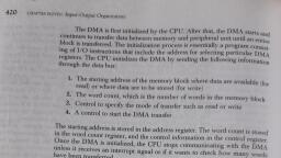
Digital Sys. &Architecture, 2., , Timer interru, This, , allows the, , are, , (MU-B.Sc. Comp), , 2-21, , generated within the, , operating system, , to, , operations on regular basis., , processor., perform certain, , incremented or decremented after every transfer based, on, , Input/output interrupts generation for, completion of Input/output operation. initiation, Input/output, failure, , number of bytes to be transferred. The counter register, , or, , Input/output, , error too can, , interrupt, 4, , Hardware, , failure, , interrupts, , failure, such as power failure or, 2.10.3 DMA, , generate, , the mode of, operation., , The data count register is used to keep a track of the, , are, , or, , Computer System, , is decremented after every transfer., , The data register is used in a special case i.e. when the, , an, , transfer of a block is to be done from one memory, location to another memory location., , are, , generated by a, memory parity error., , Also you will note in the Fig. 2.10.9 the read and write, signals are bidirectional. The DMA controller is initially, programmed by the CPU, for the count of bytes to be, , DMA stands for Direct Memory Access. The, I/0 module, can directly access (read, the, or write) memory using, this method., , transferred, address of the memory block for the data, to be transferred etc., , During this, , active, operation of the CPU, hence transfer rate is limited and, , CPU for 1/0 transfer., , (DMA, , the DMAC. This is because the CPU has to tell the DMAC, whether it is reading or writing from the DMAC., , CPU is also busy doing the transfer, the solution for these problems., over, , DMAC, , controller), the read and write lines work as inputs for, , Interrupt driven and programmed 1/0 require, , DMA controller takes, , programming of the, , operation., , DMA is, , Once the DMAC takes the control of the system bus i.e., , transfers the data between the memory and I/0 device,, these read and write signals work as output signals., , the control of the bus, fromn, , They are used to tell the memory that the DMAC wants, to read or write from the memory according to the, operation being data transfer from memory to 1/0 or, from 1/0 to memory., , The internal block diagram of a DMA controller of the, 1/0 module for DMA method of 1/0 interfacing is, shown in the Fig. 2.10.9., , The speciality of DMA is that the CPU carries on with, other work while the DMA controller deals with, transfer of data. DMA controller sends a signal when, , Data, , count, , finished., Data, , Data liness, , register, , Working of DMA, , Address, , 1., , Initially, switches S, S, and S, are at position A., , 2., , No direct access to memory; by I/0., , register, , Addresslines, DMA request-, , 3., , DMAAcknowledge, , Control, , Interrupt, , logic, , 4., , Read, Write, , are, , 5., , Using IN/OUT instruction, you can program DMA, controller chip, for various modes., , 6., , Whenever, peripheral device is ready to transfer data,, , various, , notice that there, you will, address, register and, egisters like data count, data, , Fig. 2.10.9,, , DIRECTLY to memory, it will generate REQUEST, , (DRQDMA REQUEST), to DMA controller, asking for, , register., , of the, hold the address, The address register is used to, daa, from which the, , memory location, , ansferred. There may be, multiple, , Microprocessor treats DMA controller, as 1/0 device, , ONLY, , DMA controller, ig.2.10.9: Internal block diagram of, In, , Microprocessor is MASTER of all three buses; address,, , data and control., , multiple, , addresses., , The, , to, address registers, address, , may be, , direct access., , | 7., , In response to, , (HOLD, , DRQ, DMA controller will activate, HRO, , request);, , connected, , to, , HOLD, , pin, , of, , microprocessor., , Techi, PDttc attons
Page 12 :
Computer System, , 2-22, , Digital Sys.&Architecture (MU-B.Sc.Comp.), , By activating HOLD line, DMA controller request2.10.4 DMA Transfer Modes, microprocessor, to HOLD for sometime and allow him, , Moment HOLD pin is HIGH, microprocessor ill, , There are various modes of operation used to transfer, the data between the memory and I/0 device by, the, DMA controller., , complete the present job and also active HLDA (HOLD, , The four major methods used are discussed below:, , to become a master of all three buses., , 3., , acknowledge) signal; informing, DMA controller to, DMA transtfer modes, , become master., 9., , Microprocessor tristates,, , all its buses,, , from memory and 1/0 device. Thus, , so, , total cutoff, , 1. Single transfer mode, , microprocessor, , 2. Block transfer mode, , relinquishes the buses and provides control to DMA, controller., , 3. Demand transfer mode, , 10. Now DMA controller master. It, will, is, , switches to position B., 11. DMA, , controller, , will, , position all three, , also, , generate DACK (DMA, to, Acknowledge) signal peripheral device; informing, that, direct access is allowed., , 12. Now it will, , generate address and control, will flow from memory to, 1/0 or V.V., , 11. After, , signal., , 4. Hidden transfer mode, , Fig. 2.10.11: DMA transfer modes, 1., , Single transfer mode, In, , single transfer mode, the device is programmed to, only after getting the control of, transferring one byte the control, , make one byte transfer, the system bus. After, , Data, , of the bus will be returned back to the, CPU., The word count will be decremented, and the address, , completing, , data transfer, DMA controller will, deactivate HOLD line. It also, positions, switches back to, position A, , decremented or incremented, , The, 14. Now, , microprocessor, , will, , regain the control, , over, , three buses., 15., , Microprocessor, , disadvantage, , has to wait for, extra request, , the, , The, , executing instructions fromn, or not, , advantage is that the CPU has not to remain out of, system or not having the access of, bus for, longer time, instead only for one transfer.system, , the, , master of the, , bus, is referred as DMA IDLE Cycle. When, DMA, controller gains the control, it is referred as, DMA, Active Cycle. This is about basics of DMA., , 2., , Block transfer mode, In block, , ALE, , Moroproo9seor, , Address, , BuiterData, Control bus, OA, OW, MEMW, MEMR, , Count i.e. the counter, becomes, End of Process, is, , Data bus, , bu9, , (EOP), , Memory, , Data bus, , DMA, , oontroler, , Control bus, , OR,, , OW, , MEMW, MEMR, DREO, , is, , activated by DREQ, and continues, until, , zero),, encountered., , a, , or an, , Terminal, external, , The, disadvantage is that the CPU has to remain out O, the system or not, having the access of system bus for, longer time, until all the, bytes in the, are, , Control bUrS, , HLDA HOLD, , transfer mode, the device, , (DMA Request) or software, request, making transfers during the service, , Addrees bus, , lalches, , HLDA, , in this method is that the, 1/0 device, long time after every transfer for the, , grant signals., , will start, , main program. Till DMA is inactive, , AD-AD, , a, , following each transfer., , Smart, (og. Drk, Peripheral, devico, contraller), , DACK, , Fig. 2.10.10: DMA controller Interconnection scheme, , block, , transferred., , The, is, , problem further increases, slower and the, system is, , complete, , its, , operation,, , in case if the, , thus the CPU has, , very long period in this, case., The, is, advantage that the l/0, data at a very faster, , speed., , 1/0 device, , waiting for the I/0 device to, to, , wait for, , device gets the transfer o
Page 13 :
Digitalital Sys.&Architecture, 3., , Demand transfer mode, , (MU-B.Sc. Comp.), , 2-23, Computer System, , In den, , transfers until a, encountered,, , Thus,, , making, , external EOP, ntil DREQ, goes inactive., may continue until, the, , or, , transfer, , ode, the device, Terminal Count or continues, , is, , Q.1, , 1/0 device has, , Q.2, , said to be a, trade off, between the, earlier two methods. If the 1/0, device is fast, on, enough it, , 3, , exhausted its, , data, , handling capacity., , Thus this method is, , will keep, , getting, , data and need, not wait for, extra, ime for the, request grant signals as in, the, , 5, , In, , hidden transfer mode, the DMA, controller takes over, , the, , charge, , on, , the, , rocessor does, , system bus, , not needs, , and transfers data, when, bus., system, The, , does not even realize of this, transfer, , processor, , being taken, , that, , access at, , all. It, , 7, , Q. 8, , happens mostly, , system, , between the machine, , importance, , of, , multiple bus hierarchies, suitable diagram., Arbitration? Explain any two techniques, Bus Arbitration., , Explain, , with block, , diagram, , the structure of lO, , Write short notes on, Programmed VO, Interrupt, Driven /O and DMA based /O., , Explain different data transfer techniques of DMA, , What, , are, , major requirements for an, , Write short note on :, , Explain, , Q. 11, , What is the need of DMA ?, , the DMA based data ttansfer, VO devices., , techniques of data transfer., Q. 12, a.12, , VO module ?, , Programmed Vo., , Q. 10, , place., , The processor does not needs the, system bus when it is, performing some execution of an instruction in the ALU, or certain, instructions, do not need the, bus, , the, , and, , with the help of, What is Bus, , module., , 9, , 4. Hidden transfer mode, , Explain, , Organization, , .4Explain the need of l/O module., Q.6, , Also the CPU has not to wait for, longer time in case if, the 1/0 device is slower, because, if the, 1/0 device is, slower the transfer terminate., , Computer Architecture., , of, , single, , transfer method., , Review Questions, Differentiate between Computer, , What, , are, , the, , module ?, . 13, , Write, , a, , Q.14, , What, , are, , Q. 15, , Explain, , the, , Explain, , major requirements, , note on:, , techniques for, , of, , its, , various, , Input/output, , Programmed Input/ Output., , major functions of an /O module?, , working, , configurations., , of, , DMA, , and, , its, , different, , cycles., Hence these transfers are hidden from the processor., , O00
 Learn better on this topic