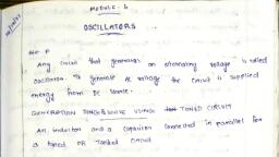
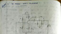
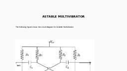
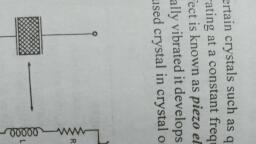
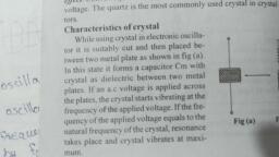
Page 1 :
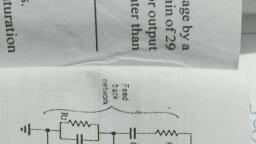
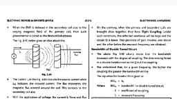
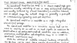
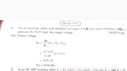
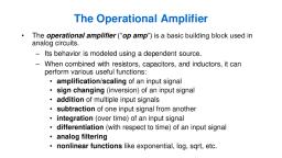
Introduction, Various branches of electronics are: Industrial electronics, Instrumentation, Communication, Power electronics etc., Various electronic circuits used in the applications of these branches are amplifiers, waveform generators, timers, various arithmetic circuits such as adder, subtractor, multipliers, Log-antilog amplifier etc., One electronic device which can be used to construct all the circuits mentioned above is called an operational amplifier or OP-AMP., OP-AMP, Voltage amplifier using a transistor uses many other components such as coupling and bypass capacitors, biasing resistors etc., In order to get higher voltage gain, we have to use more than one such amplifiers together. This will make the circuit bulky., So people started using the amplifier in the integrated circuit (IC) form., Why it is called Operational Amplifier?, An OP-AMP is basically an amplifier which could be configured to perform a variety of operations such as amplification, addition, subtraction, differentiation and integration. Hence it is called operational amplifier., OP-AMP is basically a multistage amplifier which uses a number of amplifier stages interconnected to each other in a complicated manner., Advantages of Op-Amp, Advantages of OP-AMP over conventional amplifier:, It has smaller size., Its reliability is higher than conventional amplifier., Reduced cost., Less power consumption., Easy to replace., Same OP-AMP can be used for various applications., OP-AMP Symbol and Terminals, The OP-AMP is basically a voltage amplifier with high voltage gain of 2 x 10⁵ or 106 dB., Differential Amplifier, Operational amplifier is expected to amplify the differential signal present between its two input terminals., Differential input signal (Vd):, The different between the input signals V1 and V2 is called as the differential signal Vd., ∴ Vd = V1 – V2, Common mode signal:, A common signal to both the input terminal i.e. V1 = V2 = V is called as common mode signal., Differential gain Ad:, Ad = Vo/ Vd, Ad (dB) = 20 log 10 [Vo/Vd], Common mode gain Ac:, Ac = Vo/ Vc, where Vc = (V1 + V2)/ 2, Total output voltage Vo:, Vo = Ad Vd + Ac Vc, Common Mode Rejection ratio (CMRR):, CMRR is the ability of a differential amplifier to reject the common mode signal successfully. It is also called figure of merit., ∴ CMRR = ρ = |Ad/ Ac|, Important characteristics of Ideal , OP-AMP, Infinite voltage gain (AV = ∞), Infinite input resistance (Ri = ∞), Zero output resistance (Ro = 0), Zero offset voltage:, In practical OP-AMPs a small output voltage is present even though both the inputs V1 and V2 are having zero value. This voltage is called as the offset voltage., 5. Infinite bandwidth:, Bandwidth of an amplifier is the range of frequencies over which all the signal frequencies are amplified almost equally., 6. Infinite CMRR, 7. Infinite slew rate (S = ∞):, The slew rate is defined change in output voltage occur simultaneously with the input voltage changes., 8. Zero power supply rejection ratio (PSRR = 0):, PSRR is specifies the degree of dependence of OP-AMP output, on the changes in power supply voltage., 9. Zero offset current., Block Diagram of OP-AMP, The Op-AMP consists of:, Input stage, Intermediate stage, Level shifting stage, Output stage, 1. Input stage:, The input stage must satisfy the following requirements:, It must have two inputs (inverting and non-inverting), It must provide a very high input impedance and low output impedance., It must be directly coupled amplifier and must have a very high CMRR., 2. Intermediate stage (gain stage):, The requirements of the intermediate stage is, High voltage gain., 3. Level shifting stage:, Due to the direct coupling between the first two stages, the input of level shifting stage is an amplified signal with some nonzero dc level., Level shifting stage is used to bring this dc level to zero volts with respect to ground., 4. Output stage:, Requirements of output stage:, Low output resistance, Large current sourcing capacity., Large output voltage swing., OP-AMP IC 741, This is one of the oldest and most popular OP-AMP IC., Features of IC 741:, No frequency compensation required., Short circuit protection., Offset voltage null capability., Large common mode and differential voltage ranges., No latch ups., Pin Configuration, Pin configuration:, IC 741 is 8 pin IC., Pin 1 and 5:, These pins can be used to nullify the offset voltage., Pin 2 and 3:, Pin number 2 and 3 are inverting and non-inverting inputs respectively., Pin 4 and 7:, Pin number 7 is for connecting the positive supply voltage +VCC while pin number 4 is to be connected to a negative supply voltage. Thus IC 741 needs a dual polarity power supply., Pin 6:, We get the output voltage at pin number 6., Pin 8:, Pin number 8 is a dummy pin which is not connected anywhere and hence should be left open or unconnected., Specifications:, Applications:, Inverting and non inverting amplifiers., Adder, subtractor., Integrator, differentiator circuits., Other applications such as V to I and I to V converter, precision rectifier, log, antilog amplifier etc., Differential Amplifier, The circuit below shows a generalized form of a differential amplifier with two inputs marked V1 and V2. The two identical transistors TR1 and TR2 are both biased at the same operating point with their emitters connected together and returned to the common rail, -Vee by way of resistor Re., Differential Amplifier, The circuit operates from a dual supply +Vcc and -Vee which ensures a constant supply. The voltage that appears at the output, Vout of the amplifier is the difference between the two input signals as the two base inputs are in anti-phase with each other., So as the forward bias of transistor, TR1 is increased, the forward bias of transistor TR2 is reduced and vice versa. Then if the two transistors are perfectly matched, the current flowing through the common emitter resistor, Re will remain constant., Like the input signal, the output signal is also balanced and since the collector voltages either swing in opposite directions (anti-phase) or in the same direction (in-phase) the output voltage signal, taken from between the two collectors is, assuming a perfectly balanced circuit the zero difference between the two collector voltages., This is known as the Common Mode of Operation with the common mode gain of the amplifier being the output gain when the input is zero., A differential amplifier can be arranged in the following configurations, *Dual input balanced output, * Dual input unbalanced output, *Single input balanced output, * Single input unbalanced output, Dual input balanced output is the basic differential amplifier configuration. If we use two input signals, the configuration is said to be dual input; otherwise it is single input configuration. If the output voltage is measured between the two collectors, it is referred as balanced output, because both collectors are at same potential with respect to ground. If output is measured at one of the collector with respect to ground , the configuration is called unbalanced out put., Virtual Short and Virtual Ground, Virtual short:, According to virtual short concept, both the input terminals are approximately at the same potential., The output voltage of an OP-AMP is given by,, Vo = AV x Vd, where, AV = open loop gain and, Vd = Differential input voltage, ∴ Vd = VO / AV, but AV = ∞ for an ideal op-amp and AV = 2 x 10⁵ for IC 741., ∴ for ideal op-amp, Vd = 0. Thus the potential difference between the input terminals is zero., Virtual ground:, If the non-inverting terminal of OP-AMP is connected to ground, then due to the “virtual short” existing between the two input terminals, the inverting terminal will also be at ground potential., Hence it is said to be at “virtual ground.”, Configurations of OP-AMP, An op-amp can work in two different modes:, Open loop mode 2. closed loop mode, Open loop configuration:, The open loop configuration is that there is absolutely no feedback present from the output to input., Closed loop configuration:, In closed loop configurations, some kind of feedback introduced in the circuit i.e. a part of output is returned back or fed back to the input., There are two types of feedback:, Positive or regenerative feedback, Negative or degenerative feedback, Positive feedback:, If the feedback signal or original signal are in phase with each other then it is called as the positive feed back., This feedback used in applications such as “oscillator” and Schmitt trigger., 2. Negative feedback:, If the signal fed back to the input and the original input signal are 1800 out of phase, then it is called as the negative feedback., It is used in applications such as an amplifier. Inverting Amplifier, In inverting amplifier, the signal which is to be amplified is applied at the inverting terminal of OP-AMP., The amplified output signal will be 1800 out of phase or “inverted” with the input signal., As shown in fig., input signal Vin is connected to inverting terminal via resistor R1., Feedback resistor Rf connected between output and inverting terminal and non inverting terminal connected to ground., As we know, output voltage is given by,, VO = AV x Vd, but Vd = V1 – V2, V1 = 0 since the NI (+) terminal is connected to ground. Hence as per virtual ground concept the INV (-) terminal is also at 0 V potential., ∴ V2 = 0, As Ri = ∞, the current IB2 goint into (-) terminal is zero., Hence current through R1 and Rf is same equal to I., ∴ Vin = I x R1 and VO = -I x Rf, Output voltage VO = AV x Vin, ∴ - IRf = AV x IR1, ∴ AV = -Rf /R1, The negative sign indicates that there is a phase shift of 1800 between the input and output voltages, Non- Inverting Amplifier, In non-inverting amplifier, input signal is applied to the non-inverting (+) terminal., Feedback resistor Rf is connected between output and inverting terminal., Input and output voltages are in phase with each other., For ideal Op-AMP, Ri = ∞, therefore the currents entering into both the input terminals of opamp will be zero. (I1 = I2 = 0), Therefore voltage across R1 is given by,, V2 = [R1 / (Rf + R1)] x VO, As per the virtual short concept,, V2 = V1 = Vin, ∴ Vin = [R1 / (Rf + R1)] x VO, Therefore closed loop voltage gain AV is given by,, AV = VO / Vin = (R1 + Rf) / R1, ∴ AV = 1 + (Rf / R1), The positive sign indicates that the input and output are in phase with each other and closed loop gain is always greater than unity (1)., Voltage follower, A voltage follower (also called a unity-gain amplifier, a buffer amplifier, and an isolation amplifier) is a op-amp circuit which has a voltage gain of 1., This means that the op amp does not provide any amplification to the signal. The reason it is called a voltage follower is because the output voltage directly follows the input voltage, meaning the output voltage is the same as the input voltage., For a non inverting amplifier gain Av=1+(Rf/R1), In a non inverting amplifier if Rf=R1=0, then Av=1, Therefore it acts as a voltage follower.