Page 1 :
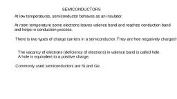
a, : SEMICONDUCTOR ELECTRONICS: MATERIALS, DEVICES, AND SIMPLE CIRCUITS, Vacuum Tubes, -, , Has two electrodes; cathode (plate) and anode, Electrons are supplied by heated cathode, Vacuum is required in the inter-electrode space so that the moving electrons don’t lose their energy upon collision, with the air molecules., Electrons only flow in one direction i.e.; from cathode to anode. Therefore, referred to as valves, Bulky, consume high power, operate generally at high voltages (~100 V) and have limited life and low reliability., Note: Vacuum tube- 2 electrodes, Triode- 3 electrodes (cathode plate and grid), Tetrode- 4 electrodes, Pentode- 5 electrodes, , Solid-state Semiconductors, - Supply and flow of charge carriers in the semiconductor devices are within the solid itself, - Are small in size, consume low power, operate at low voltages and have long life and high reliability, , Classification of Metals, Conductors and Semiconductors, On the basis of conductivity, On the basis of the relative values of electrical conductivity (σ) or resistivity (ρ = 1/σ), the solids are broadly classified, as:, 1. Metals, They possess very low resistivity (or high conductivity)., ρ ~ 10-2 – 10-8 Ω m, σ ~ 102 – 108 Sm-1, 2. Semiconductors, They have resistivity or conductivity intermediate to metals and insulators., ρ ~ 10-5 – 106 Ω m, σ ~ 105 – 10-6 S m-1, 3. Insulators, They have high resistivity (or low conductivity)., ρ ~ 1011 – 1019 Ω m, σ ~ 10-11 – 10-19 S m-1, Types of semiconductors, 1., 2., a., b., c., , Elemental semiconductors- Si and Ge, Compound semiconductorsInorganic- CdS, GaAs, CdSe, InP, etc., Organic- anthracene, doped phthalocyanines, etc., Organic polymers- polypyrrole, polyaniline, polythiophene, etc., , Band theory in Solids, -, , According to the Bohr atomic model, in an isolated atom the energy of any of its electrons is decided by the orbit in, which it revolves., But when the atoms come together to form a solid, they are close to each other. So, the outer orbits of electrons, from neighboring atoms would come very close or could even overlap.
Page 2 :
-, , -, , -, , Inside the crystal each electron has a unique position and no two electrons see exactly the same pattern of, surrounding charges. Because of this, each electron will have a different energy level., These different energy levels of electrons (when present in bulk/solid) with continuous energy variation form energy, bands., The energy band which includes the energy levels of the valence electrons is called the valence band., The energy band above the valence band is called the conduction band., With no external energy, all the valence electrons will reside in the valence band., If the lowest level in the conduction band happens to be lower than the highest level of the valence band, the, electrons from the valence band can easily move into the conduction band. Normally the conduction band is empty., But when it overlaps on the valence band electrons can move freely into it., If there is some gap between the conduction band and the valence band, electrons in the valence band all remain, bound and no free electrons are available in the conduction band., Conduction in solids on the basis of Band Theory, Let us consider what happens in the case of Si or Ge crystal containing N atoms. For Si, the outermost orbit is the, third orbit (n = 3), while for Ge it is the fourth orbit (n = 4). The number of electrons in the outermost orbit is 4 (2s, and 2p electrons). Hence, the total number of outer electrons in the crystal is 4N. The maximum possible number of, electrons in the outer orbit is 8 (2s + 6p electrons). So, for the 4N valence electrons there are 8N available energy, states., At the distance between the atoms in the crystal lattices of Si and Ge, the energy band of these 8N states is split, apart into two which are separated by an energy gap Eg., The lower band which is completely occupied by the 4N valence electrons at temperature of absolute zero is the, valence band., The other band consisting of 4N energy states, called the conduction band, is completely empty at absolute zero., The lowest energy level in the conduction band is shown as EC and highest, energy level in the valence band is shown as EV. Above EC and below EV, there are a large number of closely spaced energy levels. The gap between, the top of the valence band and bottom of the conduction band is called, the energy band gap (Energy gap Eg). It may be large, small, or zero,, depending upon the material., , Case1, When the conduction band is partially filled and the balanced band is partially empty or when the conduction and, valance bands overlap, the solid is said to be conductor. When there is overlap electrons from valence band can, easily move into the conduction band. This situation makes a large number of electrons available for electrical, conduction. When the valence band is partially empty, electrons from its lower level can move to higher level, making conduction possible. Therefore, the resistance of such materials is low or the conductivity is high.
Page 3 :
Case 2, When a large band gap Eg exists (Eg > 3 eV). There are no electrons, in the conduction band, and therefore no electrical conduction is, possible. The energy gap is so large that electrons cannot be excited, from the valence band to the conduction band by thermal excitation., Such solids are called insulators., , Case 3, When a finite but small band gap (Eg < 3 eV) exists, at room temperature, some electrons from valence band can acquire enough energy to cross, the energy gap and enter the conduction band. These electrons, (though small in numbers) can move in the conduction band. Such solids, are called semiconductors. Hence, the resistance of semiconductors is not, as high as that of the insulators., , Intrinsic Semiconductor (PYQ 2015), -, , -, , -, , -, , -, , -, , -, , -, , Consider the lattice structure of Si and Ge. These structures are called, diamond-like structures. Each atom is surrounded by four nearest, neighbors., Si and Ge have four valence electrons. In its crystalline structure, every, Si or Ge atom tends to share one of its four valence electrons with each, of its four nearest neighbor atoms, and also to take share of one electron, from each such neighbor. These shared electron pairs are referred to as, forming a covalent bond/valence bond. The two shared electrons can be, assumed to shuttle back-and-forth between the associated atoms holding, them together strongly., At low temperatures, all bonds are intact and no bond is broken. As the, temperature increases, more thermal energy becomes available to these, electrons and some of these electrons may break–away (becoming free, electrons contributing to conduction)., The thermal energy effectively ionizes a few atoms in the crystalline, lattice and creates a vacancy in the bond. The neighborhood, from which, the free electron (with charge –q) has come out leaves a vacancy with an, effective charge (+q). This vacancy with the effective positive electronic, charge is called a hole. The hole behaves as an apparent free particle with, effective positive charge., In intrinsic semiconductors, the number of free electrons (ne) is equal to, the number of holes (nh) –, , Where ni is called the intrinsic carrier concentration, In semiconductors, apart from the electrons, the holes also move. Holes, move in the direction opposite from that of motion of electrons. But,, the motion of hole is independent of the motion of free electrons and, is a way of describing the motion of bound electrons., The free electron moves completely independently as conduction, electron and gives rise to an electron current (Ie) under an applied, electric field., Under the influence of electric field, the holes move towards negative, potential and give rise to hole current (Ih), The total current is the sum of conduction current and hole current-
Page 4 :
-, , Apart from the process of generation of conduction electrons and holes,, a simultaneous process of recombination occurs in which the electrons, recombine with the holes. At equilibrium, the rate of generation is equal, to the rate of recombination of charge carriers. The recombination occurs, due to an electron colliding with a hole., , -, , An intrinsic semiconductor will behave like an insulator at T = 0 K. It is the thermal energy at higher temperatures (T, > 0K), which excites some electrons from the valence band to the conduction band. These thermally excited, electrons at T > 0 K, partially occupy the conduction band., , Extrinsic Semiconductor (PYQ 2015), -, , -, , -, , The conductivity of an intrinsic semiconductor depends on its temperature, but at room temperature its conductivity, is very low. Hence to improve their conductivity, we add certain impurities., When a few parts per million (ppm) of a suitable impurity is added to the pure semiconductor, the conductivity of, the semiconductor is increased manifold. Such materials are known as extrinsic semiconductors or impurity, semiconductors., The deliberate addition of a desirable impurity is called doping and the impurity atoms are called dopants. Such a, material is also called a doped semiconductor., The dopant has to be such that it does not distort the original pure semiconductor lattice. It occupies only a very few, of the original semiconductor atom sites in the crystal. A necessary condition to attain this is that the sizes of the, dopant and the semiconductor atoms should be nearly the same., There are two types of dopants used in doping the tetravalent Si or Ge:, (i) Pentavalent (valency 5)- Arsenic (As), Antimony (Sb), Phosphorous(P), (ii) Trivalent (valency 3)- Indium (In), Boron (B), Aluminum (Al), The pentavalent and trivalent dopants in Si and Ge give rise to two different types of semiconductors-, , -, , -, , 1. n-type Semiconductor, When an atom of +5 valency element occupies the position of an atom, in the crystal lattice of Si, four of its electrons bond with the four silicon, neighbors while the fifth remains very weakly bound to its parent atom., This is because the four electrons participating in bonding are seen as part, of the effective core of the atom by the fifth electron., As a result, the ionization energy required to set this electron free is very, small and even at room temperature it will be free to move in the lattice, of the semiconductor. Thus, the pentavalent dopant is donating one extra, electron for conduction and hence is known as donor impurity. The number, of electrons made available for conduction by dopant atoms depends strongly, upon the doping level and is independent of any increase in ambient temperature., , •
Page 5 :
-, , -, , -, , -, , -, , -, , -, , -, , On the other hand, the number of free electrons (with an equal number of holes), generated by Si atoms, increases weakly with temperature. In a doped, semiconductor the total number of conduction electrons ne is due to the electrons, contributed by donors and those generated intrinsically, while the total number, of holes nh is only due to the holes from the intrinsic source. But the rate of, recombination of holes would increase due to the increase in the number of, electrons. As a result, the number of holes would get reduced further., Thus, with proper level of doping the number of conduction electrons can be made, much larger than the number of holes. Hence in an extrinsic semiconductor doped, with pentavalent impurity, electrons become the majority carriers and holes the, minority carriers. These semiconductors are, therefore, known as n-type semiconductors., For n-type semiconductors-, , 2. p-type Semiconductors, This is obtained when Si or Ge is doped with a trivalent impurity like Al, B, In, etc., The dopant has one valence electron less than Si or Ge and, therefore, this atom, can form covalent bonds with neighboring three Si atoms but does not have any, electron to offer to the fourth Si atom. So, the bond between the fourth neighbor, and the trivalent atom has a vacancy or hole., Since the neighboring Si atom in the lattice wants an electron in place of a hole, an, electron in the outer orbit of an atom in the neighborhood may jump to fill this, vacancy, leaving a vacancy or hole at its own site. Thus, the hole is available for, conduction., Note that the trivalent foreign atom becomes effectively negatively, charged when it shares fourth electron with neighboring Si atom. Therefore, the, dopant atom of p-type material can be treated as core of one negative charge, along with its associated hole, These holes are in addition to the intrinsically generated holes while the source of, conduction electrons is only intrinsic generation. Thus, for such a material, the holes, are the majority carriers and electrons are minority carriers. Therefore, extrinsic, semiconductors doped with trivalent impurity are called p-type semiconductors., For p-type semiconductors, the recombination process will reduce the number, (ni)of intrinsically generated electrons to ne., For p-type semiconductors-, , Energy band of extrinsic semiconductors, In the case of extrinsic semiconductors, additional energy states due to donor impurities (ED) and acceptor impurities, (EA) also exist., a. n-type, ED is slightly below EC and electrons from this level move easily into the conduction band with little supply of energy, b. p-type, EA is slightly above the top of EV and with little energy electrons from valence band jump into the level EA, -
Page 6 :
The electron and hole concentration in a semiconductor in thermal equilibrium-, , Note: The crystal maintains an overall charge neutrality as the charge of additional charge carriers is just equal and, opposite to that of the ionized cores in the lattice., , p-n Junction (PYQ 2020), A p-n junction is the basic building block of many semiconductor devices like diodes, transistor, etc., p-n Junction formation, Consider a p-type semiconductor. A small part of this is converted into an n-type semiconductor by adding certain, impurities. The semiconductor now contains a n-region and p-region with a metallurgical junction between p and n, region. Two processes, diffusion and drift lead to the formation of a p-n junction as follows-, , In an n-type semiconductor, the concentration of electrons is more compared, to the concentration of holes. And in a p-type semiconductor, the concentration, of holes is more than the concentration of electrons. During the formation of p-n, junction, due to the concentration gradient across p-, and n- sides, holes diffuse, from p-side to n-side (p → n) and electrons diffuse from n-side to p-side (n → p)., This motion of charge carries gives rise to diffusion current across the junction., When an electron diffuses from n → p, it leaves behind an ionized donor on n-side., This ionized donor (positive charge) is immobile as it is bonded to the surrounding, atoms. As the electrons continue to diffuse from n → p, a layer of positive charge, (or positive space-charge region) on n-side of the junction is developed., When a hole diffuses from p → n due to the concentration gradient, it leaves behind an ionized acceptor (negative, charge) which is immobile. As the holes continue to diffuse, a layer of negative charge (or negative space-charge, region) on the p-side of the junction is developed. This space-charge region on either side of the junction together is, known as depletion region, Due to the positive space-charge region on n-side of the junction and negative space charge region on p-side of the, junction, an electric field directed from positive charge towards negative charge develops. Due to this field, an, electron on p-side of the junction moves to n-side and a hole on n-side of the junction moves to p-side. The motion, of charge carriers due to the electric field is called drift. Thus, a drift current, which is opposite in direction to the, diffusion current starts., Initially, diffusion current is large and drift current is small. As the diffusion process continues, the space-charge, regions on either side of the junction extend, thus increasing the electric field strength and hence drift current. This, process continues until the diffusion current equals the drift current. Thus, a p-n junction is formed. In a p-n junction, under equilibrium there is no net current., The n-material has lost electrons, and p material has acquired electrons. The n material is thus positive relative to, the p material. Since this potential tends to prevent the movement of electron from the n region into the p region, it, is often called a barrier potential., , -, , -, , -, , -, , -, , Important PYQs t.EE?s, ¥ Ques: How does an increase in doping concentration affect the width of depletion layer of a p-n junction diode (PYQ, 2020) [1M], ., , Ans: Decreases, , Semiconductor Diode (PYQ 2020, 2018, 2014, 2010), A semiconductor diode is a p-n junction with metallic contacts provided at the ends for the application of an external, voltage. It is a two-terminal device. The direction of arrow indicates the conventional direction of current (when the, diode is under forward bias).
Page 7 :
-, , -, , -, , -, , -, , -, , -, , -, , -, , -, , p-n junction diode under forward bias, When an external voltage V is applied across a semiconductor diode such that, p-side is connected to the positive terminal of the battery and n-side to the, negative terminal it is said to be forward biased., The direction of the applied voltage is opposite to that of the applied voltage, therefore, the width of the depletion layer decreases and the barrier height, is reduced, The I-V characteristic of a semiconductor diode under forward bias is as, shown. If the applied voltage is small, the barrier potential will be reduced, only slightly below the equilibrium value, and only a small number of carriers, in the material will possess enough energy to cross the junction. So, the, current will be small. If we increase the applied voltage significantly, the, barrier height will be reduced and a greater number of carriers will have the, required energy. Thus, the current increases., Due to the applied voltage, electrons from n-side cross the depletion region, and reach p-side (where they are minority carries). Similarly, holes from p-side, cross the junction and reach the n-side (where they are minority carries). This, process under forward bias is known as minority carrier injection., The total diode forward current is sum of hole diffusion current and, conventional current due to electron diffusion., p-n junction diode under reverse bias, When an external voltage (V) is applied across the diode such that n-side is, positive and p-side is negative, it is said to be reverse biased, The direction of applied voltage is same as the direction of barrier potential., As a result, the barrier height increases and the depletion region widens due, to the change in the electric field., The diode reverse current is not very much dependent on the applied voltage., Even a small voltage is sufficient to sweep the minority carriers from one side, of the junction to the other side of the junction. The current is not limited by, the magnitude of the applied voltage but is limited due to the concentration, of the minority carrier on either side of the junction., The current under reverse bias is essentially voltage independent up to a critical, reverse bias voltage, known as breakdown voltage (Vbr). When V = Vbr, the diode, reverse current increases sharply. Even a slight increase in the bias voltage causes, large change in the current., Summary, In forward bias, the current first increases very slowly till the, voltage across the diode crosses a certain value. After the, characteristic voltage, the diode current increases significantly, (exponentially), even for a very small increase in the diode bias, voltage. This voltage is called the threshold voltage or cut-in voltage, For the diode in reverse bias, the current is very small and almost, remains constant with change in bias. It is called reverse saturation, current. At very high reverse bias (break down voltage), the current, suddenly increases., The forward bias resistance is low as compared to the reverse bias, resistance. For diodes, we define a quantity called dynamic resistance, as the ratio of small change in voltage ∆V to a small change in current ∆I:
Page 8 :
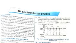
Note: 1. In forward bias, current is of the order of mA and in reverse bias, it is of the order of µA, 2. The property of diodes that forward bias resistance is low as compared to reverse bias resistance is used to rectify, ac voltages, , Important PYQs, -, , ¥i÷E÷s, , Ques: In the following diagram is the junction diode forward biased or reverse biased? (PYQ 2017) [1M], , Ans: Since the p-side is connected to a lower voltage (0V/ground) and n-side is connected to higher voltage (5V), the, junction diode is reverse biased, , Application of Junction Diode as a Rectifier (PYQ 2019, 2017, 2014, 2012, 2010), From the V-I characteristic of a junction diode we see that it allows current to pass only when it is forward biased., So, if an alternating voltage is applied across a diode the current flows only in that part of the cycle when the diode is, forward biased. This property is used to rectify alternating voltages and the circuit used for this purpose is called a, rectifier., , -, , -, , -, , -, , -, , -, , -, , Half-Wave Rectifier, If an alternating voltage is applied across a diode in series with a load, a, pulsating voltage will appear across the load only during the half cycles, of the ac input during which the diode is forward biased. Such rectifier, circuit is called a half-wave rectifier., The secondary of a transformer supplies the desired ac voltage across, terminals A and B. When the voltage at A is positive, the diode is, forward biased and it conducts. When A is negative, the diode is reverse, biased and it does not conduct., Therefore, in the positive half-cycle of ac there is a current through the, load resistor RL and we get an output voltage whereas there is no current, in the negative half-cycle. In the next positive half-cycle, again we get the, output voltage. Thus, the output voltage is restricted to only one direction, and is said to be rectified. Since the rectified output of this circuit is only, for half of the input ac wave it is called as half-wave rectifier., Full-Wave Rectifier (PYQ 2019, 2017, 2010), The circuit using two diodes gives output rectified voltage corresponding to, both the positive as well as negative half of the ac cycle. Hence, it is known, as full-wave rectifier., Here the p-side of the two diodes are connected to the ends of the secondary, of the transformer. The n-side of the diodes are connected together and the, output is taken between this common point of diodes and the midpoint of, the secondary of the transformer. So, for a full-wave rectifier the secondary, of the transformer is provided with a center tapping and so it is called, center-tap transformer., The voltage rectified by each diode is only half the total secondary voltage., Each diode rectifies only for half the cycle, but the two do so for alternate, cycles. Thus, the output between their common terminals and the center-tap, of the transformer becomes a full-wave rectifier output., Suppose the input voltage A with respect to the center tap at any instant is, positive. At that instant, voltage at B being out of phase will be negative., So, diode D1 gets forward biased and conducts (while D2 being reverse
Page 9 :
-, , -, , biased is not conducting). Hence, during this positive half cycle we get, an output current. In the course of the ac cycle when the voltage at A, becomes negative with respect to center tap, the voltage at B would be, positive. In this part of the cycle diode D1 would not conduct but diode D2, would, giving an output current and output voltage (across RL) during the, negative half cycle of the input ac. Thus, we get output voltage during both, the positive as well as the negative half of the cycle., The rectified voltage is in the form of pulses of the shape of half sinusoids., Though it is unidirectional it does not have a steady value. To get steady dc, output from the pulsating voltage, a capacitor or an inductor is connected, across the output terminals (parallel to the load RL). Since these additional, circuits appear to filter out the ac ripple and give a pure dc voltage, so they, are called filters., When the voltage across the capacitor is rising, it gets charged. If there is no external load, it remains charged to the, peak voltage of the rectified output. When there is a load, it gets discharged through the load and the voltage across, it begins to fall. In the next half-cycle of rectified output, it again gets charged to the peak value. The rate of fall of, the voltage across the capacitor depends inversely upon the product of capacitance C and the effective resistance RL, used in the circuit and is called the time constant. To make the time constant large value of C should be large. So,, capacitor input filters use large capacitors. The output voltage obtained by using capacitor input filter is nearer to, the peak voltage of the rectified voltage., , Special purpose p-n junction devices (PYQ 2020, 2019, 2018, 2015, 2014, 2010), A. Zener Diode (PYQ 2020), -, , -, , -, , It is a special purpose semiconductor diode, named after its inventor C. Zener., It is designed to operate under reverse bias in the breakdown region and used, as a voltage regulator., Zener diode is fabricated by heavily doping both p-, and n- sides of the junction. Due to this, depletion region formed, is very thin and the electric field of the junction is extremely high even for a small reverse bias voltage, The I-V characteristics of Zener diode are as followsWhen the applied reverse bias voltage(V) reaches the breakdown voltage (VZ) of, the Zener diode, there is a large change in the current. After the, breakdown voltage VZ, a large change in the current can be produced by almost, insignificant change in the reverse bias voltage. So, Zener voltage, remains constant, even though current through the Zener diode varies over a, wide range. This property of the Zener diode is used for regulating supply voltages, so that they are constant., This is because reverse current is due to the flow of electrons (minority carriers), From p → n and holes from n → p. As the reverse bias voltage is increased, the, electric field at the junction becomes significant. When the reverse bias voltage, V = VZ, then the electric field strength is high enough to pull valence electrons, from the host atoms on the p-side which are accelerated to n-side. These, electrons account for high current observed at the breakdown. The emission of, electrons from the host atoms due to the high electric field is known as internal, field emission or field ionization.
Page 10 :
Zener diode as Voltage Regulator (PYQ 2020), When the ac input voltage of a rectifier fluctuates, its rectified output also, fluctuates. To get a constant dc voltage from the dc unregulated output, of a rectifier, we use a Zener diode., The unregulated dc voltage (filtered output of a rectifier) is connected to, the Zener diode through a series resistance Rs such that the Zener diode, is reverse biased. If the input voltage increases, the current through Rs, and Zener diode also increases. This increases the voltage drop across, Rs without any change in the voltage across the Zener diode. This is, because in the breakdown region, Zener voltage remains constant even, though the current through the Zener diode changes. Similarly, if the, input voltage decreases, the current through Rs and Zener diode also, decreases. The voltage drop across Rs decreases without any change in, the voltage across the Zener diode. Thus, any increase/decrease in the, input voltage results in, increase/decrease of the voltage drop across Rs, without any change in voltage across the Zener diode. Thus, the Zener, diode acts as a voltage regulator., , B. Optoelectronic junction devices (PYQ 2019, 2018, 2015, 2013, 2010), Optoelectronic devices are those semiconductor diodes in which carriers are generated by photons (photoexcitation), (i), Photodiodes used for detecting optical signals (photodetector), (ii), Light emitting diodes (LEDs) convert electrical energy into light, (iii), Photovoltaic devices which convert optical radiation into electricity (solar cells), , -, , -, , -, , -, , 1. Photodiodes (PYQ 2019, 2018, 2015, 2013, 2010), A Photodiode is a special purpose p-n junction diode fabricated with a, transparent window to allow light to fall on the diode. It is operated, under reverse bias., When the photodiode is illuminated with light (photons) with energy, (hν) greater than the energy gap (Eg) of the semiconductor, then, electron-hole pairs are generated due to the absorption of photons., The diode is fabricated such that the generation of e-h pairs takes place, in or near the depletion region of the diode., Due to electric field of the junction, electrons and holes are separated, before they recombine. The direction of the electric field is such that, electrons reach n-side and holes reach p-side. Electrons are collected, on n-side and holes are collected on p-side giving rise to an emf., When an external load is connected, current flows. The magnitude of, the photocurrent depends on the intensity of incident light, (photocurrent is proportional to incident light intensity)., , Note: It is easier to observe the change in the current with change in the, light intensity, if a reverse bias is applied. Thus, photodiode can be used, as a photodetector to detect optical signals.
Page 11 :
Important PYQs, -, , ¥i÷E÷s, , Ques: Three photodiodes D1, D2, D3 are made of semiconductors having bandgaps of 2.5 eV, 2 eV and 3 eV, respectively. Which one of them will not be able to detect light of wavelength 600nm (PYQ 2019) [2M], Ans: The photodiode whose bandgap will be less than the energy of the most energetic photon in the light beam will, not be able to detect the light. Therefore, let us calculate the energy of photonE = hν = hc/λ, = 6.62 × 10-34 × 3× 108 / 600nm, = 2.06 eV, Therefore, D2 with a band gap of 2eV will not be able to detect the light, , -, , -, , -, , -, , 2. Light Emitting Diode (LED) (PYQ 2013), It is a heavily doped p-n junction which under forward bias emits spontaneous radiation. The diode is encapsulated, with a transparent cover so that emitted light can come out., When the diode is forward biased, electrons are sent from n → p (where they are minority carriers) and holes are, sent from p → n (where they are minority carriers). At the junction boundary the concentration of minority carriers, increases compared to the equilibrium concentration (i.e., when there is no bias)., Thus, at the junction boundary on either side of the junction, excess minority carriers are there which recombine, with majority carriers near the junction. On recombination, the energy is released in the form of photons. Photons, with energy equal to or slightly less than the band gap are emitted., When the forward current of the diode is small, the intensity of light emitted is small. As the forward current, increases, intensity of light increases and reaches a maximum. Further increase in the forward current results in, decrease of light intensity. LEDs are biased such that the light emitting efficiency is maximum., The V-I characteristics of a LED is similar to that of a Si junction diode., LEDs that can emit red, yellow, orange, green and blue light are commercially available. The semiconductor used for, fabrication of visible LEDs must at least have a band gap of 1.8 eV. The compound semiconductor Gallium Arsenide –, Phosphide (GaAs1-xPx) for making LEDs of different colors., Advantages of using LEDs, 1. Low operational voltage and less power, 2. Fast action and no warm up time required, 3. It is nearly monochromatic (small bandwidth), 4. Long life and ruggedness, 5. Fast on-off switching capability, , 3. Solar Cell, A solar cell is basically a p-n junction which generates emf when solar, radiation falls on the p-n junction. It works on the same principle, (photovoltaic effect) as the photodiode, except that no external bias, is applied and the junction area is kept much larger for solar radiation, to be incident because we are interested in more power., The generation of emf by solar cell when light falls on it is due to the, following 3 processesa. Generation of e-h pairs due to light (with hν > Eg) close to the junction, b. Separation of electrons and holes due to electric field of the depletion, region. Electrons are swept to n-side and holes to p-side, c. Collection of electrons reaching the n-side by the front contact and those reaching the p-side by back contact, Thus p-side becomes positive and n-side becomes negative giving rise to photovoltage
Page 12 :
When an external load is connected, a photocurrent IL flows through the load. The I-V characteristics are as shown-, , Note: I-V characteristics of solar cell are drawn in 4th quadrant because solar cell does not draw current but provides, it to the load., , Important criteria for making solar celli., Band gap (1-1.8eV), ii., High optical absorption, iii., Electrical conductivity, iv., Availability of raw material, v., Cost, Uses of solar cellsi., Used to power electronic devices in satellites and space vehicles, ii., Used as power supply to some calculators, , Note: Sunlight is not always required for a solar cell. Any light with photon energies greater than the bandgap will, do., , Important Definitions and Derivations, , E, , Ques: Explain the terms depletion layer and potential barrier in a p-n junction diode. How are the (a) width of, depletion layer and (b) value of potential barrier affected when p-n junction is forward biased (PYQ 2020, 2018,, 2014, 2010) [2M], Ques: (a) Draw a circuit diagram and explain the working of a Zener diode as a dc voltage regulator with the help of, its I-V characteristic, (b) What is the purpose of heavy doping a p- and n- sides of a Zener diode (PYQ 2020) [3M], Ques: Why are photodiodes required to work in reverse bias? (PYQ 2019, 2015) [1M], Ques: Explain briefly how photodiode operates (PYQ 2018, 2015, 2013, 2010) [2M], Ques: Draw the circuit diagram of a full wave rectifier and also give the input and output wave forms (PYQ 2019,, 2017, 2012, 2010) [3M], Ques: Distinguish between intrinsic and extrinsic semiconductors (PYQ 2015) [2M], Ques: Mention the important considerations required while fabricating a LED (PYQ 2013) [2M]