Page 1 :
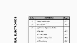
ELECTRONICS AMPLIFIERS, , , , , , , , 3.1 INTRODUCTION, , , , , , Amplifier is 2 term used to describe a circuit that produces, and enhanced version of its input signal, However, not all, amplifier circuits are identical as they're classified in line with, their circuit configurations and modes of operation., , In “Etectronics", small signal amphfiers are ordinanly used, devices as they need the power to amplify a comparatively, smal input signal, for instance from a sensor like a photodevice, into a far larger signaling to drive a relay, lamp or, electro-acoustic transducer for instance., , There are several types of electronic circuits classed as, amplifiers, from Operational Amplifiers and smatt Signal, Amplifiers up to giant Signal and Power Amplifiers, The, classification of an amplifier depends upon the dimensions of, the signal, glant or smalt, its physical configuration and the, way it processes the signal, that is the connection between, input signal and current flowing within the load., , The type or classification of an amplifier is given within the, folowing Table 3.1,, , , , 3.2 CLASSIFICATION OF SIGNAL AMPLIFIER, , , , Table 3.1, , , , Type of, Signal, , Type of, Configuration, , Classification Frequency of, , Operation, , , , [Smal Signa! [Common Emitter, , Class A Amoéfier | Oirect Current (DC), , , , Large Signal | Common Base, , Class B Ampifier | Audio Frequencies (AF), , , , ‘Common Collector |Class AB Amoéfer | Racio Frequences (RF), , , , , , Class C Amplifier | VHF, UNF and SHF, Frequencies, , , , , , , , , , , , Amplifiers are often thought of as an easy box or block, containing the amplifying device, like a Bipolar transistor,, Field effect transistor or Operational amplifier, that has two, input terminals and two output terminals (ground being, common) with the output signal being abundant larger than, that of the input because it has been “Amplified”., , 3.2.1 Ideal Amplifier, , We can know how to specify the characteristics for a perfect, amplifier fram our discussion on top of, with regards to its, Gain, that means voltage gain:, , ® The amplifiers gain, (A) should stay constant for variable, values of Input., , , , > Gain isn’t be suffering from frequency. Signals of alt, frequencies should be amplified by precisely the same, quantity., * The amplifiers gain should not add noise to the output., It should take away any noise that's already exists within, ‘the input, > The amplifiers gain mustn't be affected by changes in, temperature giving smart temperature stability., > The gain of the electronic equipment should stay stable, over long periods of your time., A signaling contains some info that can't be utilized if doesn't, have correct strength. The method of accelerating the signal, strength is named as Amplification, The majority equipment, should embody some means that for amplifying the signals., We discover the utilization of amplifiers in medical devices,, scientific instrumentation, automation, ‘military tools,, communication devices. and even in unit instrumentation, Amplification in sensible applications is finished victimization, Multi-stage amplifiers Vanety of single-stage amplifiers, square measure cascaded to make a Multi-stage amplifier., allow us to see however a single-stage electronic equipment, is constructed, that is that the basic for 2 Mult-stage, amplifier., , 3.2.2 Single-Stage Transistor Amplifier, , (3.4), , When only one transistor with associated circuitry is, employed for amplifying a weak signal, the circuit Is thought, as Singte-Stage electronic equipment., , Analyzing the operating of a Single-stage amplifier circuit, makes us straightforward to grasp the formation and dealing, of Multi-stage amplifier circuits, One stage transistor, amplifier has one transistor, bias circuit and different auxiliary, parts. The subsequent circuil diagram shows however one, stage transistor amplifier seems like., , , , , , Fig. 3.1
Page 2 :
ELECTONIC DEVICES & CIRCUITS (BATU) 432} ELECTRONICS AMPLIFIERS, , , , * When a weak input signal is gwen to the base of the Due to the presence of coupling capacitor C, the output, transistor as shown in the Fig. 3.1, a small amount of base across the resistance R. ts free from the collector's DC, current flows. Due to the transistor action a larger current voltage. If this 1s often not gift, the bias candmons of, flaws in the callectar of the transistor. (As the collector consequent stage are going to be drastically modified, current is B times of the base current which means & = Bis} because of the shunting result af RC, because it would, Now, as the collector current increases, the voltage drop are available parallel ta R; of consequent stage, across the resistor RC also Increases, wich is collected as the >» Emitter by-Pass Capacitor Cr, output. This capacitor is used in parallel to the emitter resistor, , = Hence a small input at the base gets amplified as the signal R.. The amplified AC signal is by passed through this. If, of larger magnitude and strength at the collecior outpul. this is often not present, that signal can pass through Re, Hence this transistor acts as an amplifier. that produces a voltage drop across Ry that may, , 3.2.3 Practical Circuit of a Transistor Amplifier feedback the input signal reducing the output voltage,, , «The circuit of a practical transistor amplifier is as shown >» The Load Resistance Ry, below, which represents a voltage divider biasing circuit The resistance R, connected at the autput is understood, , as Load resistance. Once variety of stages square, measure used, then R, represents the input resistance of, consequent stage., , 3.2.4 Various Circuit Currents, , , , Let us bear numerous circut currents within the complete, amplifier circuit This square measure already mentioned within, the on top of Fig. 32, © = Base Current, When no signal is applied within the base Greuil, DC base, current IB flows because of biasing circuit Once AC signal is, applied, AC base current ip additionally flaws. Therefore, with, the applying ol signal, total base current ip is given by, , , , , , , , , , , , Fig. 3.2, «The various prominent circuit elements and their functions, are as described below,, , > Biasing Circuit, , ig = gry, * Collector Current, , When no signal is applied, a DC collector current k flows due, to biasing curcut, When AC signal is applied, AC collector, , The resistors Ry, Ry and Re form the biasing and current i: also flows, Therefore, the total collector current ic is, stabilization circuit, which helps in establishing a proper given by, operating paint. ee ki, > Input Capacitor Cn Where,, Ic = Ble, , This capacitor couples the input signal to the base of the, Transistor, The input capacitor Gn allows AC signal, but, isofates the signal source from Rz. If this capacitor isn’t, present, the input signal gets directly applied, that | « Emitter Current, , zero signal collecor current, i = Bi, collecot current due to signal, , , , changes the bias at R2. When no signal is applied, a OC emitter current Ik flows. With, > Coupling Ca the application of signal, tatal emitter current iz is given by, . kt kei,, This capacitor is present at the tip of ont, ahi al ip of one stage and ft should be remembered that, connects it to the apposite stage. Because it couples two k= btk, Stages it's known as Coupling capacitor, This capacitor ie KEL, , blocks DC of one stage to enter the opposite however As base current is usually small, it is to be noted that, permits AC to pass. Thus it's additionally knawn as block kek, condenser. and wei
Page 3 :
ELECTONIC DEVICES & CIRCUITS (BATU), , These are the important considerations for the practical circuit of, transistor amplifier. Now let us know about the classification of, Amplifiers,, , An Amplifier circuit Is one which strengthens the signal. The, , amplifier action and the important considerations for the practical, , ciecurt of transistor amplifier,, , Let us now try ta understand the classificatian of amplifiers., , Amplifiers ace classified according to many considerations., , Based on Number of Stages, , Depending upon the number of stages of Amplification, there are, , Single-stage amplifiers and Multi-stage amplifiers., , ® Single-Stage Amplifiers : This has anty ane transistor circuit,, which is a single stage amplification,, , + Multi-Stage Amplifiers : This has multiple transistor circuit,, which provides multi-stage ampiification., , Based on its Output, , Depending upon the parameter that is amplified at the output,, , there are voltage and power amplifiers,, , * Voltage Amplifiers : The amplifier circuit that increases the, yoltage levet of the input signal, is called as Voltage amplifier., , * Power Amplifiers : The amplifier circuit that increases the, power level of the input signal, is called as Power amplifier., , Based on the Input Signals, , Depending upon the magnitude of the input signal applied, they, , can be categorized as Small signal and large signai amplifiers., , * Stmail Signal Amplifiers : When the input signal & so weak, $0 as to produce small fluctuations in the collector current, compared to its quiescent value, the amptifier is known as, Small signal amplifier., , + Large Signal Amplifiers : When the fluctuations in collector, current are large ie. beyond the linear portion of the, characteristics, the amplifier is known as large signal, amplifier., , Based on the Frequency Range, , Depending upon the frequency range of the signals being used,, , there are audio and radio amplifiers,, , * Audio Amplifiers : The amplfer circuit that amplifies the, signals that le in the audso frequency range ie. from 20Hz ta, 20 KHz frequency range, is called as audio amplifier,, , * Power Amplifiers = The amplifier cecuil that amplifies the, signals that lie in a very high frequency range, is called as, Power arnplifier., , Based on Biasing Conditions, , Depending upon their mode ol aperation, there are class A, class, , B and class C amplifiers., , * Class A Amplifier ; The biasing conditions in class A power, amplifier are such that the collector current flows for the, entire AC signal applied., , (3.3), , ELECTRONICS AMPLIFIERS, , © Class B Amplifier ; The biasing conditions in class B power, amplifier are such that the collector current flows for halfcycle of Input AC signal applied,, , © Class € Amplifier : The brasing conditions in class C power, amplifier are such that the collector current fiows lor less, than half cycle of input AC signal apphed, , © Class AB Ampilfier : The class AB power amplifier 5 one, which Is created by combining both class A and class B mn, order to have all the advantages of both the classes and 10, minimize the problems they have., , Based on the Caupling Method, , Depending upon the method of couphng one stage to the other,, , there are RC coupled. Transformer coupled and direct coupled, , amplifier, , * RC Coupled Amplifier : A Multi-stage amplifier circuit that is, coupled to the next stage using resistor and capacitor (RC}, combination can be called as a RC coupled amplifier,, , © Transformer Coupled Amplifier ; A Multi-stage amplifier, Grcuit that is coupled to the next stage, with the help of a, tansformer, can be called as a Transformer coupled, amplifier., , @ Direct Coupled Amplifier : A Multi-staqe amptifier circuit, that is coupled to the next stage directly, can be called as a, direct coupled amplifier,, , Based on the Transistor Configuration, , Depending upon the type of transistor configuration, there are CE, , CB and CC amplifiers., , ¢ CE Amplifier ; The amplifier circuit that is formed using a CE, configured transistor combination 1s called as CE amplifier,, , ® CB Amplifier : The amplifier circuit that is formed using a CB, configured transistor combination is called as CB ampleier., , e@ CC Amplifier: The amphifier cwcurl thal & formed using a CC, canfigured transistor combination ss called as CC amplifier,, , * Any transistor amplifier, uses a transistor to amplify the, signals which is connected in one of the three configurations., For an amplifier it is a better state to have a high input, impedance, in order to avoid loading effect in Multi-stage, circuits and lower output impedance, in order to deliver, Maximum output to the load. The voltage gain and power, gain should also be high to produce a better output., , «Let us now study different configurations to understand, which configuration suits better for a transistor to work as an, amplifier., , 3.2.5 CB Amplifier, , , , , , * «The amplifier circuit that is formed using a CB configured, transistor combination is called as CB amplifier.
Page 4 :
ELECTONIC DEVICES & CIRCUITS (BATU) (3.4), , Construction, , The common base ampiifier circuil using NPN transistor is as, shown below, the input signal being applied at emitter base, junction and the output signal being taken from collector, base junction., , , , , , , , , , Fig. 3.4, The emitter base junction is forward biased by Ver and, collector base junction is reverse biased by Vcc. The, operating point is adjusted with the help of resistors Re and, Ry. Thus the values of I. Ib and kn are decided by Yec, Vite, Re, and Re, Operation, @ When no input is applied, the quiescent conditions are, formed and na output is present. As Vb, Is at negative with, respect to ground, the forward bias 15 decreased, for the, positive half of the input signal As a result of this, the base, current Ip also gets decreased, , , , , , , , , , ¢ The below Fig. 3.4 shows the CB amplifier with self-bias, circuit,, Voc, gr, tt Re, Sn EE, KG, Fe, SR, PLZ ontout, 3, r, Fig. 34, * As we know that,, k = &= Bl, , Both the collector current and emitter current get decreased., The voltage drop across RC is, Ve = kRe, This ¥c also gets decreased., As [Ry decreases, ¥cq Increases. Its because,, Vow = Yee = TcRe, , , , 3.2., , ELECTRONICS AMPLIFIERS, , Thus, a positive half cycle output ss produced,, , In CB configuration, a positive input produces a positive, output and hence input and output are in phase. So, there is, no phase reversal between input and output in a, CB amplifier., , If CB configuration is considered for amplification, it has low, input impedance and high output impedance. The voltage, gain is also low compared to CE configuration. Hence CB, configured amplifiers are used at high frequency, applications., , 6 CE Amplifier, , , , The amplifier circuit Lhat is formed using a CE configured, transistor combination is called as CE amplifier., , , , , , , , , , , , , , , , , , , , Construction, * = The common emitter amplifier circuit using NPN transistor is, a5 shown below, the input signal being applied at emitter, base junction and the output signal being taken from, collector base junction, Vee, ", SR, an, Fn tp? ea *, I 1, ~°, pi SR,, +, Fig. 3.5, * The emitter base junction is forward biased by Vie and, collector base juncton is reverse biased by Vcc. The, operating point is adjusted wth the help of resistors Re and, R.. Thus the values of L, kb and fp are decided by Vcc, Ver Re, and Re,, Operation, , When oo input is applied, the quiescent conditions are, formed and no output is present. When positive half of the, signal is being applied, the voltage between base and emitter, Vee iS increased because It is already positive with respect lo, ground., , As forward bias increases, the base current too increases, accordingly Since Iy = ily, the collector current increases as, well., , The following circurt diagram shows a CE amplifier with selfbias creut.
Page 5 :
ELECTONIC DEVICES & CIRCUITS (BATU), , , , , , , , , , , , , , , , , , Fig, 3.6, , * = The collector current when flows through Az, the vohage, drop increases,, , Ve # KRe, , = As aconsequene of this, the voltage between collector and, , emitter decreases, Because,, Vea = Veo = Re, , * Thus, the amplified voltage appears across Re,, , » Therefore, in @ CE amplifier, as the postive going signal, appears as a negatve going signal, it is understood that, thera «sa phase shift of 180° between input and output,, , * CE amplifier has a high inpul impedance and lower output, impedance than C8 amplifier The voltage gain and power, gain are also high in CE ampiher and hence this is mostly, used in Audio amplifiers,, , 3.2.7 CC Amplifier, , © = The ampliher circuit that Is formed using a CC configured, wansistor combination |s called as CC amplifier,, Construction, , 43.5), , ELECTRONICS AMPLIFIERS, , «The emitter base junction |s forward biased by ¥i¢ and, collector base Junction |s reverse biased by cc. The Q-values, of ly and I, are adjusted by Ry and Re,, , Operation, , = When no input is applied, the quiescent conditions are, formed and no output is present, When positive half of the, signal is being applied, the forward bias is increased because, Voe is positive with respect to collector or ground, With this,, the base current fg and the collector current Ic are increased., , * The following circuit diagram shows a CC amplifier with selfbias circuit., , , , , , cae She, , , , , , Fig. 3.8, , © Consequently, the voltage drop across R, ie. the outpul, voltage is increased. As a result, positive half cycle is, obtained. As the input and output are In phase, there is no, phase reversal, , * CC configuration ss considered for amplification, though CC, amphher has betier input impedance and lower output, impedance than CE amplifier, the yaltage gain of CC is very, fess which kemuts its applications ta Impedance matching only., , 3.2.8 Comparison between CB, CE and CC Amplifiers, , , , «© Let us compare the characteristic details of CB, CE, and CC, , , , , , , , , , , , , , , , amphfers., Table 3.2, * The common collector amplifier circuit using NPN transistor Characteristic ce ce ce, is a5 shown below, the input signal being applied at base Ingpul resistance Low Yery low High, coflectar junction and the output signal being Laken from (1K 2K) | (25-1500) | (20-SOOKM, emitter collector junction, ‘Oulput resistance Large High low, (=50K) | (= 500K} | {50-1000KO}, Current gain B righ act Fgh (1 + BI, Voltage gein High High Less than one, (= 1500) f= 1500), Power galn High High Low, (= 10,0001] [# 7500) (250 - $00}, Phase balwaen haut and outpd | reversed sania same, , , , , , , , , , , , , , , , , , , , Fig. 3.7, , , , , , * Due to the compatibility and characteristic features, the, cammon-emitter configuration |s mostly used in amplifier, circuits.