Notes of EEE 1styr GP Chunar Mzp22, ECD ECD syllabus.pdf - Study Material
Page 1 :
72, 2.5 ELECTRONIC COMPONENTS & DEVICES, (Common With Electronics Engineering), L T P, 6 - 6, RATIONALE, Knowledge of Electronic components & devices is quite essential for a student of electronic, engineering diploma programme. With the knowledge of these active and passive components he, will work successful in every field of the branch. Therefore a diploma student in electronics, engineering must be equipped with the fundamental knowledge about electronic components,, voltage and current source, semi conductor diode, transistors and FET for successful handling of, industrial problems., LEARNING OUTCOMES, After undergoing the subject, the student will be able to:, • Indentify and distinguish between active components (BJT, FET etc) and passive, components (Resistor, Capacitor, inductor etc)., Understand voltage and current sources as well as their interconversions., Understand the working and application of semiconductor diode including half wave, rectifier & Full wave rectifier., Understand the working of BJT and hence able to design amplifier using it., Compare various transistors biasing circuit and stabilize their operating points., Understand the working of FET and hence able to design amplifier using it., Compare BJJT, JFET, MOSFET & CMOS., DETAILED CONTENTS, 1., Introduction to Electronics, (06 Periods), Application of electronic in different fields., Brief introduction to active components and devices., 1.1, 1.2, 2., Passive Components, (12 Periods), 2.1. Resistor- Working characteristics/properties, Resistors-Carbon film, metal-film,, (presets and potentiometers), carbon composition, wire wound and variable typ, constructional details, characteristics (size, voltage, tolerance temperature and, noise consideration, specification, Testing, mutual, frequency dependence), comparison and typical applications, Voltage Dependent Resistor (VDR)., APPROVED IN CDC COMMITTEE MEETING,OF BTE,UP, LKO DATED:26-09-2021, 1
Page 2 :
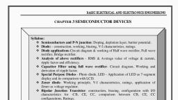
73, 2.2. Capacitors- Working characteristics/properties, Capacitors-polyester, Metalized, polyester, ceramic paper mica and electrolytic tantalum and solid aluminium types;, construction details and testing, specifications, mutual comparison & typical, applications., 2.3. Inductors, Transformers and RF coils- Working characteristics/properties Methods of, manufacture of inductors, RF coils and small power and AF transformer and their, testing, Properties of cores, Needs and type of shielding., 3., Voltage And Current Sources, (06 Periods), 3.1. Concept of constant voltage sources, symbol and graphical representation,, characteristics of ideal and practical voltage sources., 3.2. Concept of constant current source, symbol and graphical representation, characteristics, of ideal and practical current sources., 3.3 Conversion of voltage sources into a current sources and vice-versa., 3.4 Concept of floating and grounded D.C. supplies., 4., Semiconductor Diode, (12 Periods), 4.1. P-N junction diode, Mechanism of current flow in P-N junction, drift and diffusion, currents, depletion layer, potential barriers, P-N junction diode characteristics,, Zener& avalanche breakdown, Concept of junction capacitance in forward &, reverse bias conditions., 4.2. Semiconductor diode characteristics, dynamic resistance & their calculation from diode, characteristics, dynamic resistance of diode in terms of diode current, Variation of, leakage current and forward voltage with temperature (No derivations)., 4.3 Diode (P-N Junction) as rectifier, Half wave rectifier, full wave rectifier including bridge, rectifier, relationship between D.C output voltage and A.C input voltage, rectification, efficiency and ripple factor for rectifier circuits, filter circuits- shunt capacitor, series, inductor, bleeder resistance, working of the filter and typical application of each type, 4.4. Different types of diodes, characteristics and typical application of power diodes, zener, diodes, varactor diodes, point contact diodes, tunnel diodes, LEDS and photo diodes, 4.5. Important specification of rectifier diode and zener diode., 5., Introduction to Bipolar Transistor:, (12 Periods), 5.1. Concept of bipolar transistor as a two junction three terminal device having two kinds, of charge carriers, PNP an NPN transistor, their symbol and mechanism of current flow,, explanation of fundamental current relations, Concept of leakage current, effect of, temperature on leakage current, Standard notation for current and voltage polarity., 5.2. CB, CE and CC configurations., APPROVED IN CDC COMMITTEE MEETING,OF BTE,UP, LKO DATED:26-09-2021, 2
Page 3 :
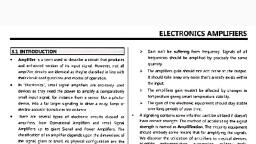
74, a. Common base configuration (CB): input and output characteristics,, determination of transistor parameters (input and output) dynamic resistance,, current amplification factor., b. Common emitter configuration (CE): current relations in CE configuration,, collector current in term of base current and leakage current (ICEO) relationship, between the leakage current in CB and CE configuration, input and output, characteristics, determination of dynamic input and output resistance and current, amplification, factor, from, the, characteristics., c. Common collector configuration (CC): Expression for emitter current in terms, of base current and leakage current in CC configuration., 5.3. Comparison of CB and CE configuration with regards to dynamic input and output, resistance, current gain and leakage current performance of CE configuration for low, frequency voltage amplification, Typical application of CB configuration in, amplification., 5.4. Transistor as an amplifier in CE configuration., a. DC load line, its equation and drawing it on collector characteristics., b. Determination of small signal voltage and current gain of basic transistor, amplifier using CE output characteristics and DC load line, Concept of power, gain as a product of voltage gain and current gain., 6., Transistor Biasing And Stabilization Of Operating Point, (09 Periods), 6.1. Different transistor biasing circuits for fixing the operating points, effect of temperature, on operating point., Need and method for stabilization of operating point., Effect of fixing operating point in cut-off or saturation region on performance of, amplifier, 6.2. Calculation of operating point for different biasing circuits, use of Thevenin's theorem, in analyzing potential divider biasing circuit., 6.3. Simple design problems on potential divider biasing circuits., Single Stage Transistor Amplifier, (09Periods), 7., 7.1. Analysis of Single Stage CE, CB and CC amplifier., 7.2. Single stage CE amplifier circuits with proper biasing components., 8., Field Effect Transistor (Fet), (06 Periods), APPROVED IN CDC COMMITTEE MEETING,OF BTE,UP, LKO DATED:26-09-2021, 3
Page 4 :
75, 8.1. Construction, operation, characteristics and Biasing of Junction FET., 8.2. Analysis of Single Stage CS,CG and CD amplifiers. (Only Brief Idea), 9., MOSFET, (06 Periods), 9.1 Construction, operation, Characteristics and Biasing of MOSFET in both depletion, and enhancement modes., 9.2 Analysis of Single Stage CS, CG and CD amplifiers. (Only Brief Idea), 10., СMOS, (06 Periods), 10.1 Construction, operation and Characteristics of CMOS in both depletion and, enhancement modes., 10.2 Use of CMOS as Invertor, Different application of CMOS, CMOS IC., 10.3 Comparison of JEET, MOSFET and Bipolar Transistor., LIST OF PRACTICALS, 1. Identification of types of packages, terminals and noting different ratings using data books, for various types of semiconductor diodes (Germanium, point contact, silicon low power,, high power and switching diode)., 2. Familiarization with lab instruments (Multi-meter/CRO), etc., 3. Testing of various passive and active components., 4. Plotting of forward V-1 characteristics for a point contact and P-N junction diode (Silicon &, Germanium diode)., 5. To Plot forward and reverse V-I characteristics for a zener diode., 6. Rectifier circuits using semiconductor diode, measurement of input and output voltage and, plotting of input and output wave shapes., i) Half wave rectifier, ii) Full wave rectifier (centre tapped and bridge rectifier circuits), 7. To Plot wave shapes of a full wave rectifier with shunt capacitor, series inductor and filter, circuit., 8. To Plot the input and output characteristics and calculation of parameters of a transistor in, common base configuration, 9. To Plot input and output characteristics and calculation of parameters of a transistor in, common emitter configuration., APPROVED IN CDC COMMITTEE MEETING,OF BTE,UP, LKO DATED:26-09-2021, 4
Page 5 :
76, 10. Transistor Biasing circuits, i) Measurement of operating point (Ic&Vce) for a fixed bias circuit., ii) Potential divider biasing circuits., (Measurement can be made by changing the transistor in the circuits by another of a same, type number)., 11. Plot the FET characteristics and determination of its parameters from these characteristics., 12. Measurement of voltage gain at 1 KHZ for different load resistance for a BJT amplifier, circuit., 13. Measurement of voltage gain for a JFET amplifier circuit., 14. Measurement of voltage gain for a MOSFET amplifier circuit., INSTRUCTIONAL STRATEGY, Electronic Components & Devices being a fundamental subject, it needs to be handled very carefully, and in a manner such that students develop clear understanding of the related concepts and, principles. The teacher may lay more emphasis on laboratory work and give home assignments to, students to inculcate self study and problem solving abilities amongst them., MEANS OF ASSESSMENT, Class Tests, Home Assignments, Attendance, Sessional Test, RECOMMENDED BOOKS, 1., Bhargava, Kulshreshttha& Gupta - "Basic Electronics& Linear Circuits" - Tata Mc-, graw-Hill., Malvino, A. P.-"Electronics Principles" -Tata Mcgraw-Hill, Robert.L.Boylestad – "Electronic Devices & Circuits Theory" – Pearson Publication., V.K.Mehta- “Principles of electronics"- S.Chand Publication., e-books/e-tools/relevant software to be used as recommended by AICTE/ NITTTR,, Chandigarh., 2., 3., 4., 5., APPROVED IN CDC COMMITTEE MEETING OF OTE LIDIvODATrna
 Learn better on this topic