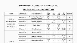
Page 1 :
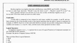
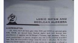
Unit 2-Logic Gates, , IntroductionIn digital electronics logic gates are very important. They are, basic circuits of digital electronics. Logic gate perform mathematical, operations like addition, Multiplication and complement. By using, logic gate, we also construct combinational circuit. It also includes, Boolean laws., Logic Gate-, , Above Figure shows logic gate which has 1 or many inputs but, only 1 output. Different terms used in logic gate are truth table,, Boolean equation and symbol etc., 1)Logic Gate-(Definition)- It is digital circuit which has 1 or many, input but only 1 output., 2)Truth table- It is a table in which logic is expressed by taking all, possible combinations of input and respective output. If there ae 2, inputs then there are 22=4 combinations of input., If there ae 2 inputs then there are 23=8 combinations of input., 3)Boolean EquationIt is mathematical equation, which represent particular gate for input, and output., , 1|Kadam A. S.
Page 2 :
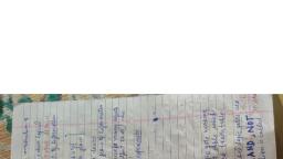
4)SymbolEach gate is represented by logic symbol., , Types of logic gateA]Basic gates1)OR gate, 2)AND gate, 3)NOT gate/INVERTER gate, B]Derived gates1)NOR gate, 2)NAND gate, 3)EX-OR gate/X-OR gate, 4)EX-NOR gate/X-NOR gate, , A]Basic gates1)OR gate-, , 2|Kadam A. S.
Page 3 :
Truth TableA, B, Y=A+B, 0, 0, 0, 0, 1, 1, 1, 0, 1, 1, 1, 1, Above figure shows symbol for OR gate. It is used to perform, mathematical operation like addition. OR gate has 2 or many inputs, but only 1 output., Truth table for OR gate is shown above from truth table we, conclude that if any 1 input is high then output is also high., IC number of OR gate is 7432, Boolean equation for OR gate- Y=A+B, , 2)AND gate-, , Truth TableA, B, Y=A B, 0, 0, 0, 0, 1, 0, 1, 0, 0, 1, 1, 1, Above figure shows symbol for AND gate. It is used to perform, mathematical operation like multiplication. AND gate has 2 or many, inputs but only 1 output., 3|Kadam A. S.
Page 4 :
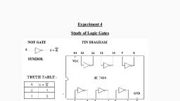
Truth table for AND gate is shown above from truth table we, conclude that in AND gate if all inputs are high (1) then output is high, (1). When any input is zero (0) then output will be zero (0), IC number of OR gate is 7408, Boolean equation for OR gate- Y=, , 3)NOT gate-, , A, 0, 1, , Y= A, 1, 0, , Above figure shows symbol for NOT gate. It is used to perform, mathematical operation like complement. NOT gate has 1 input and, only 1 output. NOT gate is also called as inverter., Truth table for NOT gate is shown above from truth table we, conclude that we get complement of given input., IC number of OR gate is 7404, Boolean equation for OR gate- Y= A, , B]Derived gatesDerived gates are constructed by using two or more basic gates., , 4|Kadam A. S.
Page 5 :
1)NOR gate-, , Truth TableA, , B, , Y=̅̅̅̅̅̅̅̅, , 0, 0, 1, 0, 1, 0, 1, 0, 0, 1, 1, 0, Above figure shows symbol for NOR gate. It is combination of, 2 basic gates i.e. OR gate and NOT gate. NOR gate has many inputs, but only one output. It also called as complement of OR gate., Truth table for NOR gate is shown above. From truth table we, conclude that when any input is high (1) then output goes low (0)., IC number of OR gate is 7402, Boolean equation for OR gate-, , 5|Kadam A. S., , ̅̅̅̅̅̅̅̅
Page 6 :
2)NAND gate-, , Truth TableA, , B, , Y=̅̅̅̅̅̅, , 0, 0, 1, 0, 1, 1, 1, 0, 1, 1, 1, 0, Above figure shows symbol for NAND gate. It is combination, of 2 basic gates i.e. AND gate and NOT gate. NAND gate has many, inputs but only one output. It also called as complement of AND gate., Truth table for NAND gate is shown above. From truth table we, conclude that when all inputs are high (1) then output goes low (0)., Otherwise output will be high (1)., IC number of OR gate is 7400, Boolean equation for OR gate- Y=̅̅̅̅̅̅, , 3)EX-OR gate/X-OR gate-, , 6|Kadam A. S.
Page 7 :
Truth TableA, , Y= A ⊕ B, , B, , 0, 0, 0, 0, 1, 1, 1, 0, 1, 1, 1, 0, Above figure shows symbol for EX-OR gate. It is combination, of 3 basic gates in which there are 2 NOT gate, 2 AND gate and 1 OR, gate. It is also called as X-OR gate., Truth table for EX-OR gate is shown above. From truth table we, conclude that if there is odd number of 1 then output will be high (1)., And if both inputs are 0 or 1 then output will be zero., IC number of OR gate is 7486, Boolean equation for OR gate- Y=A ⊕ B, Y= ̅, , 7|Kadam A. S., , ̅
Page 8 :
4)EX-NOR, , gate-, , Truth TableA, , Y=̅̅̅̅̅̅̅, ⊕, , B, , 0, 0, 1, 0, 1, 0, 1, 0, 0, 1, 1, 1, Above figure shows symbol for EX-NOR gate. It is combination, of 2 gates in which there are 1 NOT gate, 1 X-OR gate. It is also, called as X-NOR gate., Truth table for X-NOR gate is shown above from truth table we, conclude that when there is even number of 1‟s then the output will be, high (1) and when all inputs are 0 then output will be 1., IC number of OR gate is 74266, Boolean equation for OR gate- Y=̅̅̅̅̅̅̅̅, ⊕, ̅, ̅, Y=̅̅̅̅̅̅̅̅̅̅̅̅̅̅̅̅̅, Y=( ̅, 8|Kadam A. S., , ̅)
Page 9 :
Demorgan’s TheoremsThese theorems are used for interchange one gate by, another proper gate. These theorems also help to simplify, complicated Boolean equation., There are 2 Demorgan’s TheoremsDemorgan’s 1st TheoremStatementThe complement of sum is equal to product of, complements., Boolean Equation̅̅̅̅̅̅̅̅̅= ̅ ̅, , 9|Kadam A. S.
Page 11 :
Proof for Demorgan’s 1st theoremSr. L.H.S., No., 1, Eqn=̅̅̅̅̅̅, 2, , 3, , R.H.S., Eqn= ̅, , Truth Table-, , ̅, , Truth Table-, , A, , B, , Y=̅̅̅̅̅̅, , A, , B, , Y= ̅, , 0, 0, 1, 1, , 0, 1, 0, 1, , 1, 1, 1, 0, , 0, 0, 1, 1, , 0, 1, 0, 1, , 1, 1, 1, 0, , Hence, Demorgan‟s 2nd Theorem is proved., ̅̅̅̅̅̅̅̅= ̅, , ̅, , 11 | K a d a m A . S ., , ̅
Page 12 :
Boolean Algebra: Rules for Boolean Algebra1)Commutative Law –, A B=B A, A+B=B+A, 2)Associative Law –, A + (B + C) = (A + B) + C = A + B + C, A(B C) = (A B)C = A B C, , 3)Distributive Law A(B + C) = A B + A C (OR Distributive Law), A + (B C) = (A + B) (A + C) (AND Distributive Law), 4)Other Basic Rules1)A + A = A, 2)A A = A, 3) ̅ ̅, 4) ̿, 5) ̅, 7) ̅, 8) 0 + A = A, 9) 1 A = A, 10) 1 + A = 1, 11) 0 A = 0, 12 | K a d a m A . S .
Page 13 :
12) ̅, 13) A + A B = A, 14) A (A + B) = A, ̅, 15), 16), , ̅, , 17)AB+ ̅, , ̅, , 18)A ̅, 19)A+( ̅, , ), , 20)(A+B)(A+C)=A+BC, 21)De Morgan's Theorem1) ̅̅̅̅̅̅̅̅̅= ̅ ̅, 2) ̅̅̅̅̅̅̅̅= ̅, , ̅, , By using above rules for Boolean algebra, we can solve any, Boolean equation in its simple form and also, we can draw logic, diagram for it., , Rules for verification and its Logic diagram 1)A+AB=A, L.H.S.=A+AB, =A(1+B), =A(1), =A, L.H.S.=R.H.S., A+AB=A, , A, 13 | K a d a m A . S ., , A
Page 14 :
2)A (A+B)=A, L.H.S.=A (A+B), =AA+AB, =A+AB, =A(1+B), =A(1), =A, L.H.S.=R.H.S., A (A+B)=A, , A, , A, , 3)A ̅̅̅̅, , AB, , L.H.S.= A ̅̅̅̅, =A ̅+AB, =0+AB, =AB, L.H.S.=R.H.S., A ̅̅̅̅, 𝐀, , 𝐁, , AB, , 14 | K a d a m A . S .
Page 16 :
L.H.S.=R.H.S., A̅, , B=A+B, , 6)A+( ̅ B)=A+B, L.H.S.= A+( ̅ B), =A, , ̅, , ), ̅, , =A, =A, , ̅̅̅, , =B(A+̅̅̅) +A, =B(1)+A, =B+A, =A+B, L.H.S.=R.H.S., A+( ̅ B)=A+B, , 16 | K a d a m A . S ., , )
Page 17 :
7)(A+B)(A+C)=A+BC, L.H.S.= (A+B)(A+C), =AA+AC+BA+BC, =A+AC+BA+BC, =A(1+C)+BA+BC, =A(1)+BA+BC, =A+BA+BC, =A(1+B)+BC, =A(1)+BC, =A+BC, L.H.S.=R.H.S, (A+B)(A+C)=A+BC, , Examples-Reduce the following equation & draw logic diagram for it., 1)ABC+A ̅ C+AB ̅, ABC+A ̅ C+AB ̅, =AC(B+ ̅ )+ AB ̅, =AC(1)+ AB ̅, =AC+ AB ̅, =A(C+B ̅), 17 | K a d a m A . S .
Page 18 :
2)AB+A(B+C)+B(B+C), AB+A(B+C)+B(B+C), = AB+AB+AC+BB+BC, =AB+AC+B+BC, =B(1+B)+AC+BC, =B(1)+AC+BC, = B+AC+BC, =B(1+C)+AC, =B(1)+AC, = B+AC, , 3), , 18 | K a d a m A . S .
Page 19 :
4), , 19 | K a d a m A . S .
Page 20 :
20 | K a d a m A . S .
Page 21 :
Karnaugh‟s Map-(K-Map)For simplification of Boolean equation, we can use Boolean, Algebra law, identities, and theorems. But Boolean Algebra method, has some disadvantages. These disadvantages are minimising by, using K-Map. The K-map is graphical representation of Boolean, equation with minimum chances of error., In „n‟ variables K-Map there are 2n cells. Each cell corresponds, to one of the combinations of variable. In each K-map there are all, possible values of variables. Gray code is used for identification., The Truth table used for expression which are in the form of1)Sum of Product (SOP), 2)Product of Sum (POS), , Examples of SOP1)A+AB+ABC, 2) ̅, , ̅, , ̅, , SOP (Sum of Product)Logical equation in sum of product form can be represented on, K-map by entering “1” in the cell of K-Map., On the other hand, product of sum (POS) form can be, represented on K-Map by entering “0” in the cell of K-Map., Each term in SOP equation is called as minterm and in POS it is, maxterm., Minterm and MaxtermFor two binary variables A and B & its complement ̅ & ̅ ., These variables are represented for all possible combinations as,, (AB), ( ̅ ),(A ̅ ),( ̅ ̅ ), 21 | K a d a m A . S .
Page 22 :
Because there are two variables 22=4 combinations are possible., , 1)Minterm-(standard product)When each combination of binary variable is ANDed then each, of this individual term is called as minterm., Minterm is represented by mi where i represent decimal, equivalent of natural binary number., 2)Maxterm-(standard sum)When each combination of binary variable is ORed then each of, this individual term is called as maxterm., Maxterm is represented by Mi where i represent decimal, equivalent of natural binary number., Below table shows minterm for three binary variables. A, B, C,, i.e. 2 =8 combinations are possible., 3, , A, 0, 0, 0, 0, 1, 1, 1, 1, , Binary Variable, B, 0, 0, 1, 1, 0, 0, 1, 1, , C, 0, 1, 0, 1, 0, 1, 0, 1, , Minterm, Product, Designation, ̅̅ ̅, m0, ̅ ̅, m1, ̅ ̅, m2, ̅, m3, ̅ ̅, m4, ̅, m5, ̅, m6, m7, , Boolean equation can be written by considering only those, minterm for which output is “1” and taking the OR of all such terms., , 22 | K a d a m A . S .
Page 23 :
ExampleIn m0, m1, m5, m7 are one then Boolean equation can be written, as follows,, Y= m0+m1+m5+m7, Y= ̅ ̅ ̅ + ̅ ̅ + ̅ +, Y=(∑, , ), , OR, Y=∑, Where, i denote the number of product terms in truth table., This configuration is called as Sum of product (SOP), K-map for sum of product (SOP)K-map is usual display of fundamental product for sum of, product. The K-map is composed of an arrangement of adjacent boxes, called as cells. Each cell represents possible combination of binary, variables in product form., There are 3 K-map structure which are usually used1) For 2-variable in K-mapIt will have 22=4 cells., 2) For 3-variable in K-mapIt will have 23=8 cells., 3) For 4-variable in K-mapIt will have 24=16 cells., Below figures shows K-map for sum of product., 1)For 2-variable in K-mapA/B, ̅, A, , ̅, ̅ ̅ (0), A ̅ (2), , 23 | K a d a m A . S ., , B, ̅B (1), AB (3)
Page 25 :
̅, 1, 1, 0, 0, , AB/C, ̅̅, ̅B, AB, A̅, Y=(∑, , C, 1, 0, 0, 1, , ), , Grouping of cellsThe cells are forming Pairs, Quads, Octet to solve the equation., 1)PairsWhen K-map shows pairs of 1 then the pair of one can eliminate, one variable, which changes its state., Example1)Pairs in 3 variable K-mapAB/C, ̅̅, ̅B, AB, A̅, , ̅, 0, 0, 0, 0, , C, 1, 1, 0, 0, , Above K-map shows pair of 1‟s the equation will be,, Y=̅ ̅ + ̅B, Above equation will be reduced to Y= ̅ C, Because the variable changes its form B to ̅, , 2) Pairs in 4 variable K-mapEg (1)-, , 25 | K a d a m A . S .
Page 31 :
3)OctetIt is possible to have group of 8 adjacent one‟s is called as octet., An octet eliminates 3 variables and gives output. An octet can, also consider as two Quads, which is shown in below K-Map., ̅̅, 0, 0, 0, 0, , AB/BC, ̅̅, ̅B, AB, A̅, , ̅, 1, 1, 1, 1, , ̅, 0, 0, 0, 0, , CD, 1, 1, 1, 1, , In above K-map 3 variable changes change state, (i.e. A to ̅ , B to ̅, C to ̅ ). Hence only one variable will appear at, the output., Y=D., Logic Diagram̅, , D, AB/BC, ̅̅, ̅B, AB, A̅, , ̅̅, 1, 1, 0, 0, , ̅, 1, 1, 0, 0, , CD, 1, 1, 0, 0, , ̅, 1, 1, 0, 0, , In above K-map 3 variable changes change state, (i.e. B to ̅, C to ̅ D to ̅ ). Hence only one variable will appear at, the output., Y=̅, Logic Diagram31 | K a d a m A . S .
Page 32 :
A, , Y= ̅, , Simplification of sum of product equationFor simplification of any equation by using K-Map, we have to, follow following steps., Step 1Find Minterms of equation., Step 2Draw K-map for minterms or equation., Step 3Form possible pair, quad or octet from k-map., Step 4Then write reduced Boolean equation by eliminating variables, which, are changing its state., Step 5Draw the equivalent logic diagram for simplified equation or reduced, equation., , Example, Solve the following equations by using k-map and draw equivalent, logic diagram., 1)Y=A̅ ̅ +AB ̅ + ̅ ̅ ̅ +̅ ̅, SolutionStep 1Minterms for the equation, 32 | K a d a m A . S .
Page 34 :
Step 2K-map for above equationThere are 3 variables, so we have to draw 3 variable K-map., AB/C, ̅̅, ̅B, AB, A̅, , ̅, 1, 0, 0, 1, , C, 1, 1, 0, 1, , Step 4In above K-map two variables changes its state (i.e. A to ̅ , C to ̅ ), =̅, In above K-map two variables changes its state (i.e. B to ̅), =̅C, Y= +, Y=̅+ ̅C, , Step 5-Logic Diagram, , 34 | K a d a m A . S .
Page 39 :
Introduction to logic familyBased on semiconductor devices digital integrated, circuit (IC) are commercially available for many digital functions., IC‟s are in different form; each form is referred as logic family., Types of logic familyA)Unipolar Logic family1)PMOS(P-Channel Metal Oxide Semiconductor), 2)NMOS(N-Channel Metal Oxide Semiconductor), 3)CMOS(Complementary Metal Oxide Semiconductor), , B)Bipolar Logic familya)Saturated bipolar logic family1)RTL(Resistor Transistor Logic), 2)DCTL(Direct Coupled Transistor Logic), 3) L(Integrated Injection Logic), 4)DTL(Diode Transistor Logic), 5)TTL(Transistor Transistor Logic), 6)HTL(High Threshold Logic), , b)Non-Saturated bipolar logic family1)ECL(Emitter Coupled Logic), 2)STTL(Schottky Transistor Transistor Logic), , According to level of integration or number of gates on the IC chip, they are classified as follows-, , 39 | K a d a m A . S .
Page 41 :
1)Propagation Delay TimeThis is used to specify speed of digital circuit. The, delay time is measured between 50% voltage level of input and output, waveform., 2)Figure of MeritFigure of merit is multiplication of speed and time., 3)FAN IN and FAN OUTFAN IN means number of inputs to the gate and FAN, OUT means number of similar gates which can be driven by output., 4)Noise MarginIn electronic circuit, electronic and magnetic field may, induce unwanted voltage this is known as Noise., The circuit which has ability to tolerate noise signal is, referred as noise immunity and measurement of immunity is called as, Noise Margin., 5)Power DissipationThis is amount of power dissipated on IC. The, standard TTL gate has power dissipation about 10 m watt. It may vary, because of signal level., 6)Current and Voltage Parametera), , –(High level input voltage), This is minimum voltage which is referred by gate as, , Logic-1, b), , –(Low level input voltage), This is maximum voltage which is referred by gate as, , Logic-0, , 41 | K a d a m A . S .
Page 42 :
c), , –(High level output voltage), , This is minimum voltage available at output, corresponding to Logic-1, d), , –(High level output voltage), , This is maximum voltage available at output, corresponding to Logic-0, , Tristate LogicIn normal circuit there are only 2 states of the output, i.e. high (1) and low (0)., In complex digital system like microcomputer and, microprocessor there are number of gate input and output required to, be connected to common like called as bus. The bus is driven by, number of gate input, but this has following drawbacks1)One or more output can be connected together, it is not possible, because of very large current from the supply and the heating of IC, may damage it., 2)Output can be connected together externally but this causes loading, and speed of operation decreases., To overcome these problems the circuit in which there is one, or more state of input is developed. This is called as Tristate or High, impedance state. This state is addition of low and high state. This, circuit is also known as TSL (Tristate Logic)., , NAND gate as Universal building blockIn digital electronics logic gate perform different operations,, but NAND gate and NOR gate have universal property that means by, using these gates we can construct all basic gates. Therefore, NAND, gate and NOR gate are called as universal building block., 42 | K a d a m A . S .
Page 43 :
43 | K a d a m A . S .
Page 44 :
TTL NAND gate-, , TTL means Transistor Transistor Logic. In digital electronics, NAND gate is called as Universal building block. IC 7400 is used to, perform NAND gate operation., Here, in above figure there is 2 input NAND gate i.e. there is, multiple emitter input transistor. Each emitter acts as input to the, NAND gate., and, are acting as 2 input AND gate. The, remaining circuit acts as invertor (NOT gate). Therefore, the above, circuit is acting like 2 input NAND gate., , The advantage of this circuit is that its low output impedance., The circuit operation is as follow1)If A and B are low (0) then, saturate. Therefore base voltage of, reduces to 0 and, is cut off. Hence, is also cut off. Under this, condition diode, will forward bias and output becomes high (1)., 2)When A and B are high (1) then collector diode of, is conducted, at that time, and, are saturated which produces low output., Without diode, acts as reverse bias. Therefore output becomes low, (0)., , 44 | K a d a m A . S .
Page 45 :
Truth table for NAND gateA, , B, , Y=̅̅̅̅̅̅, , 0, 0, 1, 1, , 0, 1, 0, 1, , 1, 1, 1, 0, , ------------------------------------------------------------------------------------, , 45 | K a d a m A . S .