Notes of BCS II, Computer Organization & Computer Organization Unit 2 memory organization.pdf - Study Material
Page 1 :
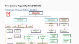
UNIT II, Memory Organization, 12-1 MEMORY HIERARCHY, Memory hierarchy in a computer system :, Memory hierarchy system consists of all storage devices employed in a computer system from the, slow but high capacity auxiliary memory to a relatively faster main memory, to an even smaller and faster cache, memory accessible to the high speed processing logic., , Figure12- 1 illustrates the components in a typical memory hierarchy. At the bottom of the hierarchy are, the relatively slow magnetic tapes used to store removable files. Next are the Magnetic disks used as backup storage., The main memory occupies a central position by being able to communicate directly with CPU and with auxiliary, memory devices through an I/O process. Program not currently needed in main memory are transferred into, auxiliary memory to provide space for currently used programs and data., The cache memory is used for storing segments of programs currently being executed in the CPU., The I/O processor manages data transfer between auxiliary memory and main memory. The auxiliary memory has a, large storage capacity is relatively inexpensive, but has low access speed compared to main memory. The cache, memory is very small, relatively expensive, and has very high access speed. The CPU has direct access to both, cache and main memory but not to auxiliary memory.
Page 2 :
12 – 2 MAIN MEMORY, Main memory is the central storage unit in a computer system. It is a relatively large and fast, memory used to store programs and data during the computer operation. The principal technology used for the main, memory is based on semi conductor integrated circuits. Integrated circuits RAM chips are available in two possible, operating modes, static and dynamic., , , , Static RAM – Consists of internal flip flops that store the binary information., Dynamic RAM – Stores the binary information in the form of electric charges that are applied to, capacitors., , Most of the main memory in a general purpose computer is made up of RAM integrated circuit chips, but a, portion of the memory may be constructed with ROM chips., , , Read Only Memory –Store programs that are permanently resident in the computer and for tables of, constants that do not change in value once the production of the computer is completed., , The ROM portion of main memory is needed for storing an initial program called a Bootstrap, loader., , , , Boot strap loader –function is start the computer software operating when power is turned on., Boot strap program loads a portion of operating system from disc to main memory and control is then, transferred to operating system., , RAM and ROM CHIP, , , RAM chip –utilizes bidirectional data bus with three state buffers to perform communication with CPU
Page 3 :
The block diagram of a RAM Chip is shown in Fig.12-2. The capacity of memory is 128 words of eight, bits (one byte) per word. This requires a 7-bit address and an 8-bit bidirectional data bus. The read and write inputs, specify the memory operation and the two chips select (CS) control inputs are enabling the chip only when it is, selected by the microprocessor. The read and write inputs are sometimes combined into one line labelled R/W., The function table listed in Fig.12-2(b) specifies the operation of the RAM chip. The unit is in operation, only when CS1=1 and CS2=0.The bar on top of the second select variable indicates that this input is enabled when it, is equal to 0. If the chip select inputs are not enabled, or if they are enabled but the read or write inputs are not, enabled, the memory is inhibited and its data bus is in a high-impedance state. When CS1=1 and CS2=0, the, memory can be placed in a write or read mode. When the WR input is enabled, the memory stores a byte from the, data bus into a location specified by the address input lines. When the RD input is enabled, the content of the, selected byte is placed into the data bus. The RD and WR signals control the memory operation as well as the bus, buffers associated with the bidirectional data bus.
Page 4 :
A ROM chip is organized externally in a similar manner. However, since a ROM can only read, the data, bus can only be in an output mode. The block diagram of a ROM chip is shown in fig.12-3. The nine address lines in, the ROM chip specify any one of the512 bytes stored in it. The two chip select inputs must be CS1=1 and CS2=0, for the unit to operate. Otherwise, the data bus is in a high-impedance state., Memory Address Map, The interconnection between memory and processor is then established from knowledge of the size of, memory needed and the type of RAM and ROM chips available. The addressing of memory can be established by, means of a table that specify the memory address assigned to each chip. The table called Memory address map, is a, pictorial representation of assigned address space for each chip in the system., , The memory address map for this configuration is shown in table 12-1. The component column specifies, whether a RAM or a ROM chip is used. The hexadecimal address column assigns a range of hexadecimal equivalent, addresses for each chip. The address bus lines are listed in the third column. The RAM chips have 128 bytes and, need seven address lines. The ROM chip has 512 bytes and needs 9 address lines., Memory Connection to CPU:, RAM and ROM chips are connected to a CPU through the data and address buses. The low order lines in, the address bus select the byte within the chips and other lines in the address bus select a particular chip through its, chip select inputs.
Page 5 :
The connection of memory chips to the CPU is shown in Fig.12-4. This configuration gives a memory, capacity of 512 bytes of RAM and 512 bytes of ROM. Each RAM receives the seven low-order bits of the address, bus to select one of 128 possible bytes. The particular RAM chip selected is determined from lines 8 and 9 in the, address bus. This is done through a 2 X 4 decoder whose outputs go to the CS1 inputs in each RAM chip. Thus,, when address lines 8 and 9 are equal to 00, the first RAM chip is selected. When 01, the second RAM chip is select,, and so on. The RD and WR outputs from the microprocessor are applied to the inputs of each RAM chip. The, selection between RAM and ROM is achieved through bus line 10. The RAMs are selected when the bit in this line, is 0, and the ROM when the bit is 1. Address bus lines 1 to 9 are applied to the input address of ROM without going, through the decoder. The data bus of the ROM has only an output capability, whereas the data bus connected to the, RAMs can transfer information in both directions.
Page 6 :
It consists of a memory array and logic for m words with n bits per word. The argument, register A and key register K each have n bits, one for each bit of a word. The match register M has m bits, one for, each memory word. Each word in memory is compared in parallel with the content of the argument register. The, words that match the bits of the argument register set a corresponding bit in the match register. After the matching, process, those bits in the match register that have been set bindicate the fact that their corresponding words have, been matched. Reading is accomplished by a sequential access to memory for those words whose corresponding bits, in the match register have been set.
Page 9 :
12-5 CACHE MEMORY, , , , , , , Effectiveness of cache mechanism is based on a property of computer programs called “locality of, reference”, The references to memory at any given time interval tend to be confined within a localized areas, Analysis of programs shows that most of their execution time is spent on routines in which instructions are, executed repeatedly These instructions may be – loops, nested loops , or few procedures that call each other, Many instructions in localized areas of program are executed, repeatedly during some time period and reminder of the program is accessed infrequently This property is, called “Locality of Reference”., , Locality of Reference, Locality of reference is manifested in two ways :, 1. Temporal- means that a recently executed instruction is likely to be executed again very soon., The information which will be used in near future is likely to be in use already( e.g. reuse of, information in loops), 2. Spatial- means that instructions in close proximity to a recently executed instruction are also likely to be, executed soon, If a word is accessed, adjacent (near) words are likely to be accessed soon ( e.g. related data, items (arrays) are usually stored together; instructions are executed sequentially, )
Page 10 :
3. If active segments of a program can be placed in afast (cache) memory , then total execution time can be, reduced significantly, 4. Temporal Locality of Reference suggests whenever an information (instruction or data) is needed first , this, item should be brought in to cache, 5. Spatial aspect of Locality of Reference suggests that instead of bringing just one item from the main, memory to the cache ,it is wise to bring several items that reside at adjacent addresses as well ( ie a block of, information ), Principles of cache, , The main memory can store 32k words of 12 bits each. The cache is capable of storing 512 of these words, at any given time. For every word stored , there is a duplicate copy in main memory. The Cpu communicates with, both memories. It first sends a 15 bit address to cahache. If there is a hit, the CPU accepts the 12 bit data from cache., If there is a miss, the CPU reads the word from main memory and the word is then transferred to cache., , , , , , , , When a read request is received from CPU,contents of a block of memory words containing the location, specified are transferred in to cache, When the program references any of the locations in this block , the contents are read from the cache, Number of blocks in cache is smaller than number of blocks in main memory, Correspondence between main memory blocks and those in the cache is specified by a mapping function, Assume cache is full and memory word not in cache is referenced, Control hardware decides which block from cache is to be removed to create space for new block containing, referenced word from memory, Collection of rules for making this decision is called “Replacement algorithm ”, , Read/ Write operations on cache, Cache Hit Operation, CPU issues Read/Write requests using addresses that refer to locations in main memory, Cache control circuitry determines whether requested word currently exists in cache, If it does, Read/Write operation is performed on the appropriate location in cache (Read/Write Hit ), Read/Write operations on cache in case of Hit, , , , In Read operation main memory is not involved., In Write operation two things can happen.
Page 11 :
1. Cache and main memory locations are updated, , simultaneously (“ Write Through ”) OR, , 2. Update only cache location and mark it as “ Dirty or Modified Bit ” and update main memory location, at the time of cache block removal (“ Write Back ” or “ Copy Back ”) ., , Read/Write operations on cache in case of Miss Read Operation, , , When addressed word is not in cache Read Miss occurs there are two ways this can be dealt with, 1. Entire block of words that contain the requested word is copied from main memory to cache and the, , particular word requested is forwarded to CPU from the cache ( Load Through ) (OR), 2. The requested word from memory is sent to CPU first and then the cache is updated ( Early Restart ), , Write Operation, , , , , If addressed word is not in cache Write Miss occurs, If write through protocol is used information is directly written in to main memory, In write back protocol , block containing the word is first brought in to cache , the desired word is then, overwritten., , Mapping Functions, , , , Correspondence between main memory blocks and those in the cache is specified by a memory mapping, function, There are three techniques in memory mapping, 1. Direct Mapping, 2. Associative Mapping, 3. Set Associative Mapping, , Direct mapping:, A particular block of main memory can be brought to a particular block of cache memory. So, it is not flexible., , In fig 12-12. The CPU address of 15 bits is divided into two fields. The nine least significant bits constitute, the index field and remaining six bits form the tag field. The main memory needs an address
Page 12 :
that includes both the tag and the index bits. The number of bits in the index field is equal to the number of address, bits required to access the cache memory., , The direct mapping cache organization uses the n- bit address to access the main memory and the k-bit, index to access the cache. Each word in cache consists of the data word and associated tag. When a new word is first, brought into the cache, the tag bits are stored alongside the data bits. When the CPU generates a memory request,, the index field is used the index field is used for the address to access the cache. The tag field of the CPU address is, compared with the tag in the word read from the cache. If the two tags match, there is a hit anfd the desired data, word is in cache. If there is no match, there is a miss and the required word is read from main Memory.
Page 13 :
In fig 12-14, The index field is now divided into two parts: Block field and The word field. In a 512 word cache there, are 64 blocks of 8 words each, since 64X8=512. The block number is specified with a 6 bit field and the word with in, the block is specified with a 3-bit field. Th etag field stored within the the cache is common to all eight words of the, same block., Associative mapping:, , In this mapping function, any block of Main memory can potentially reside in any cache block, position. This is much more flexible mapping method. In fig 12-11, The associative memory, stores both address and content(data) of the memory word. This permits any location in cache to, store any word from main memory.The diagram shows three words presently stored in the cache., The address value of 15 bits is shown as a five-digit ctal number and its corresponding 12-bit, word is shown as a four-digit octal number. A CPU address of 15-bits is placed in the argument, register and the associative memory is searched for a matching address. If address is found, the, corresponding 12-bit data is read and sent to the CPU. If no match occurs, the main memory is, accessed for the word.
Page 14 :
Set-associative mapping:, In this method, blocks of cache are grouped into sets, and the mapping allows a block of main memory to, reside in any block of a specific set. From the flexibility point of view, it is in between to the other two methods., , The octal numbers listed in Fig.12-15 are with reference to the main memory contents. When, the CPU generats a memory request, the index valus of the address is used to access the cache., The tag field of the CPU, , address is then compared with both tags in the cache to determine if a match occurs. The, comparison logic dine by an associative search of the tags in the set similar to anassociative, memory search thus the name “Set Associative”., Replacement Policies, , , , , When the cache is full and there is necessity to bring new data to cache , then a decision, must be made as to which data from cache is to be removed, The guideline for taking a decision about which data is to be removed is called, replacement policy Replacement policy depends on mapping, There is no specific policy in case of Direct mapping as we have no choice of block, placement in cache Replacement Policies, , In case of associative mapping, , , , A simple procedure is to replace cells of the cache in round robin order whenever, a new word is requested from memory, This constitutes a First-in First-out (FIFO) replacement policy, , In case of set associative mapping, , , , , Random replacement, First-in First-out (FIFO) ( item chosen is the item that has been in the set longest), Least Recently Used (LRU)( item chosen is the item that has been least recently, used by CPU)
Page 15 :
12-6 VIRTUAL MEMORY, , , , , Early days memory was expensive – hence small, Programmers were using secondary storage for overlaying, Programmers were responsible for breaking programs in to overlays , decide, where to keep in secondary memory, arranging for transfer of overlays, between main memory and secondary memory, , Virtual Memory - Background, , , , , , Separate concept of address space and memory locations, Programs reference instructions and data that is independent of available physical, memory Addresses issued by processor for Instructions or Data are called Virtual, or Logical addresses, Virtual addresses are translated in to physical addresses by a combination of, Hardware and Software components, , Types of Memory, , , , Real memory, , Main memory, Virtual memory, Memory on disk, , Allows for effective multiprogramming and, tight constraints of main memory, , relieves the user of, , Address Space and Memory Space, , , , , Address used by a programmer is called virtual address and set of such addresses, is called address space, Address in main memory is called a location or physical address and set of such, locations is called the memory space, The Address Space is allowed to be larger than the memory space in computers, with virtual memory
Page 16 :
In a multiprogramming computer system, programs and data are transferred to and from, auxiliary memory and main memory based on demands imposed by the CPU. Suppose that, program1 is currently, being executed in the CPU. Program1 and a portion of its associated data are moved from, auxiliary memory into main memory as shown in fig. 12-16. Portions of programs and data need, not be in contiguous locations in memory since information is being moved in out, and empty, spaces may be available in scattered locations in memory., , In fig 12-17, To map a virtual address of 20 bits to a physical address of 15 bits. The mapping is a, dynamic operation, which means that every address is translated immediately as a word is referenced by, CPU. The mapping table may be stored in a separate memory. In first case, an additional unit is required, as well as one extra memory access time. In the second case, the table takes space from main memoy and, two accesses to memory are required with program running at half speed. A third alternative is to use an, associative memory. Address Mapping Using Pages, The physical memory is broken down into groups of equal size called blocks, which may, range from 64 to 4096 word each. The term page refers to groups of address space of the same, size. Portions of programs are moved from auxiliary memory to main memory in records equal, to the size of a page. The term “page frame” is sometimes used to denote a block.
Page 17 :
In fig 12-18, a virtual address has 13 bits. Since each page consists of 1024 words, the high order three bits, of virtual address will specify one of the eight pages and the low order 10 bits give the line address within the page., , The organization of the memory mapping table in a paged system is shown in Fig.12-19. The memory, page table consists of eight word , one for each page. The address in the page tabledenotes the page, number and the content of the word gives the block number where that page is stored in main memory., The table shows that pages 1,2,5 and 6 are now available in main memory in blocks 3,0,1 and 2,, respectively.
Page 18 :
Associative Memory Page Table, A random-access memory page table is inefficient with respect to storage utilization., , Replace the random access memory-page table with an associative memory of four words, as shown in Fig12-20. Each entry in the associative memory array consists of two fields. The, first three bits specify a field for storing the page number. The last two bits constitute a field for, storing the block number. The virtual address is placed in the argument register., Address Translation, , , A table is needed to map virtual address to a physical address ( dynamic, operation) This table may be kept in, a separate memory or, main memory or, associative memory
Page 19 :
12-7 MEMORY MANAGEMENT HARDWARE
Page 20 :
A memory management system is a collection of hardware and software procedure for managing the, various programs residing in memory. The memory management software is part of an overall operating system, available in many computers., The basic components of a memory management unit are:, , A segment is a set of logically related instructions or data elements associated with a given name. Segment, may be generated by the programmer or by the operating System. The address generated by segmented program is, called a logical address. The logical address may be larger than the physical memory address as in virtual memory,, but it may also be equal, and sometimes even smaller than the length of the physical memory address., Segmented –Page Mapping, The property of logical space is that it uses variable-length segments. The length of each segment is, allowed to grow and contract according to the needs of the program being executed.
Page 21 :
T, , Translation Look aside Buffer, , , , , , The mapping tables may be stored in two separate small memories or in main memory. A memory, reference from the CPU will require three access to memory., o One to fetch the page table, o One to fetch the data, o From main memory, To overcome this problem a high-speed cache is set up for page table entries., Called a Translation Look aside Buffer (TLB).
Page 22 :
, , , , , Contains page table entries that have been most recently used., If page table entry is present (TLB hit), the frame number is retrieved and the real address is, formed., If page table entry is not found in the TLB (TLB miss), the page number is used to index the, process page table., First checks if page is already in main memory If not in main memory a page fault is issued The, TLB is updated to include the new page entry., , Numerical Example, Consider the 20 bit logical address specified in Fig.12-22(a). The 4 bit segment number specifies one of 16, possible segments. The 8 bit page number can specify up to 256 pages, and the b-bit word field implies a page size, of 256 words., The physical memory shown in Fig 12-22(b) consists of 220 words of 32 bit each. The 20 –bit address, is divided into two fields: a 12-bit block number and an 8 bit word number. Thus, physical, memory, is, divided into 4096, blocks, of 256, words each., , Consider a program loaded into memory that requires five pages. The operating system may assign to this, program segment 6 and pages 0 through 4, as shown in Fig 12-23(a). the total logical addressrange for the programis, fromhexadecimal 60000 to 604FF. when the program is loaded into physical memory , it is distributed among five, blocks in physical memory where the operating system finds empty spaces. The correspondence between each, memory block and logical page number is then entered in a table as shown in Fig.12-23(b).
Page 24 :
(a) Seyment and gage table mappin, , Segment, , Page, , Block, , 6, , 02, , 019, , _, , _, , _, , A6l, , 6, , (b) Associative memory (TLB), , Figure 12-24 Logical to physical memory mapping example (all numbers are, in hexadecimal)., , Introduction to USB Storage Device:A USB flash drive which is also known as a thumb drive or pen drive, is a portable storage, device that uses flash memory. It is small enough to be carried anywhere with you. Instead of a compact, disk, a flash drive can be used. When a user connects a flash memory device to a computer’s flash port, the, operating system recognizes it as a removable drive and then a drive is assigned to it. Universal serial bus, is used to store files and data copies to run diagnostics to troubleshoot device issues, or to boot an, operating system. The drives are compatible with Microsoft Windows, Linux, MacOS, various Linux, variants, and a variety of BIOS boot ROMs. In this article, a detailed introduction to Universal serial bus is, given that what is USB, its uses and types?, Here are two types of memory are available to store the data volatile and non-volatile. USB flash drive, comes under the non-volatile category. It has to resort to power to save, transfer, and put the data into it., However, it can also store the data into it without a power supply also. It will transmit the memory, command in the form of an electronic signal to the internal circuit. Even if there is no supply of power, it, can store the data without any harm or data loss. It maintains the integrity of the data. It does not have any, moving parts. Through USB it can be compatible with all devices. When we plug in the pen drive into a, computer USB port, the device starts reading, writing,, Uses of USB, For secure storage of data, software, and application files., , , Personal data transport., , , , To update motherboard firmware.
Page 25 :
, , For booting operating systems, , , , Computer forensics and law enforcement., , , , Operating system installation media., , , , To backup the data., , , , Windows ReadyBoost., , , , Application carriers., , , , Media storage and Marketing., , , , Audio players., , , , Product or brand promotion., features :1. It uses less power and does not have any fragile moving parts., 2. Data storage on this device is impervious to mechanical shock, magnetic field, and dust. These, properties of USB flash drive make them suitable to move from one place to another., 3. It can store more data compared to other devices, 4. Some USB flash drives are specially manufactured suing rough rubber and metal to provide the, waterproof feature and make it hard. This type of drive does not lose their memory after hung, submerged in the water.
 Learn better on this topic