Page 1 :
BASIC ELECTRICAL AND ELECTRONICS ENGINEERING, , CHAPTER 3 SEMICONDUCTOR DEVICES, , Syllabus:, Semiconductors and P-N junction: Doping, depletion layer, barrier potential., Diode: - construction, working, biasing, V-I characteristics, ratings., Diode applications-Circuit diagram & working of Half wave rectifier, Full wave, rectifier, Bridge rectifier., Analysis of above rectifiers - RMS & Average value of voltage & current,, ripple factor and efficiency., Capacitor Filter using full wave rectifier- Circuit diagram, Working and, derivation of ripple factor., Special Purpose Diodes - Photo diode, LED - Application of LED as 7-segment, display and its comparison with LCD., Zener diode- Working principle, V-I characteristics, ratings, application of, Zener as voltage regulator., Bipolar Junction Transistor- construction, biasing, configuration with I/O, characteristics for -CB, CE, CC, comparison between CB, CE, CC, configurations, Ratings., Application of transistor - CE amplifier, BJT as switch., Special Purpose Transistors- Photo transistor, , 2.1 INTRODUCTION:, Insulator:, An insulator is material that offers a very low level of conductivity when a voltage is, applied., Example: Rubber, glass, wood etc., Conductor:, The term conductor is applied to any material that will support a generous flow of, charge when a voltage source is applied across its terminals, Example: Copper, Al, salt solutions, etc., Semiconductor:, A semiconductor is a material that has a conductivity level somewhere between the, extremes of an insulator and a conductor., Inversely related to the conductivity of material is its resistivity which is used to, compare the resistance level of materials., In terms of energy bands, semiconductors are those substances in which the forbidden, gap is narrow., Example: Silicon, germanium, Gallium, arsenide etc.
Page 2 :
BASIC ELECTRICAL AND ELECTRONICS ENGINEERING, , Typical Resistivity Values:, , Properties of Semiconductor:, 1) It acts insulator at absolute zero temperature i.e. number of free carriers is zero., 2) As temperature increases its conductivity increases i.e. resistivity decreases., Energy Band Diagrams:, , Semiconductor is material that has a conductivity level between the extremes of an, insulator and a conductor., Some of the unique qualities of Ge & Si are due to their atomic structure., Semiconductor materials such as Ge and Si that show a reduction in resistance with increase in, temperature are said to have a negative temperature coefficient., The atoms of both materials form a very definite pattern that is periodic in nature. (i. e., continually repeats itself)., Both Ge & Si have 4 electrons in outermost (valence) shell., In a pure Ge or Si crystal these 4 valence electrons are bonded 4 adjoining atoms., Semiconductor Types:, a) Intrinsic semiconductor (Pure semiconductor), b) Extrinsic semiconductor (Impure semiconductor), i., N- type semiconductor, , ii., , a) Intrinsic semiconductor:, Intrinsic semiconductors are pure semiconductors., , P - type semiconductor
Page 3 :
BASIC ELECTRICAL AND ELECTRONICS ENGINEERING, , The free electrons in the material due to only to natural causes are known as intrinsic, carriers., Valence electrons can absorb kinetic energy from natural cases like light energy &, thermal energy & break the covalent bonds to become free., An increase in temperature of a semiconductor results in an increase in the number of, free electrons in the material., Semiconductor Ge & Si have a negative tempt. Coefficient as their resistance, decreases with increase in temperature., At 0ºK all the semiconductors are acting as pure insulators because at 0ºK all the, states in the conduction band are empty., In case of intrinsic semiconductor the no. of electrons in the conduction band is, equals to the no. of holes in the valence band., Thus in intrinsic semiconductor both electrons and holes are present. When the, electrical field is applied then the electrons move towards the anode & holes towards, the cathode., Hence total conductivity of semiconductor is sum of the conductivities due to holes, and electrons., Thus a semiconductor in which electrons and holes are solely created by the thermal, excitation is called „Intrinsic semiconductor’., b) Extrinsic Semiconductor:, The characteristics of pure or intrinsic semiconductor materials can be altered, significantly by addition of certain impurity atoms into the pure semiconductor, material., The impurities are (1) Pentavalent materials like Antimony, Phosphorus, Arsenic., (2) Trivalent materials like Boron, Gallium, Indium., Impurities are added to 1 part in 10 million., Addition of these impurities can totally change the electrical properties of the, semiconductor material., When certain impurity atoms like antimony and boron are added to a pure, semiconductor material, we get an „Extrinsic Semiconductor‟., As a result of this doping we get extrinsic semiconductor., Doping:, The process of adding certain impurity like Antimony or Boron into pure semiconductor, like Silicon is called „Doping Process’., Types of Extrinsic Semiconductors:, a) N-type semiconductor, , b) P-type semiconductor, , a) N-type Semiconductor:, To increase the number of conduction-band electrons in intrinsic silicon,, pentavalent impurity atoms are added. These are atoms with five valence electrons such, as arsenic (As), phosphorus (P), bismuth (Bi), and antimony (Sb)., As illustrated in Figure, each pentavalent atom (antimony, in this case) forms, covalent bonds with four adjacent silicon atoms. Four of the antimony atom‟s valence, electrons are used to form the covalent bonds with silicon atoms, leaving one extra, electron. This extra electron becomes a conduction electron because it is not involved in, bonding. Because the pentavalent atom gives up an electron, it is often called a donor, atom. The number of conduction electrons can be carefully controlled by the number of, impurity atoms added to the silicon. A conduction electron created by this doping process
Page 4 :
BASIC ELECTRICAL AND ELECTRONICS ENGINEERING, , does not leave a hole in the valence band because it is in excess of the number required to, fill the valence band., , Majority carriers Electrons, Minority Carriers Holes, , Figure: Antimony impurity in n-type material, b) P-type semiconductor:, To increase the number of holes in intrinsic silicon, trivalent impurity atoms are, added. These are atoms with three valence electrons such as boron (B), indium (In), and, gallium (Ga). As illustrated in Figure, each trivalent atom (boron, in this case) forms, covalent bonds with four adjacent silicon atoms., , Majority Carriers Holes, Minority Carriers Electrons
Page 5 :
BASIC ELECTRICAL AND ELECTRONICS ENGINEERING, , Figure: Boron impurity in p-type material, Conductivity of semiconductor:, Fundamental difference between a metal and a semiconductor., Metal is unipolar. (Conducts current by means of charges of sign only i.e. electrons.), Semiconductor is bipolar. (Contains two charge carrying particles of opposite sign- holes, and electrons) (holes-positive charge, electron-negative charge), P-N Junction:, , The PN junction is formed from a n-type and p-type semiconductor material., In p-region the holes are majority carriers and electrons are minority carriers, whereas in, n-region electrons are majority carriers and holes are minority carriers., Free electrons on the n-side and free holes on the p-side can initially diffuse across the, junction. Uncovered charges are left in the neighborhood of the junction.
Page 6 :
BASIC ELECTRICAL AND ELECTRONICS ENGINEERING, , The diffusion of electrons and holes stop due to the barrier p.d (p.d across the junction), reaching some critical value., The barrier p. d. (or the contact potential) depends on the type of semiconductor,, temperature and doping densities., At room temperature, typical values of barrier potential difference are:, Ge ~ 0.2 – 0.4 V, Si ~ 0.6 – 0.8 V, , Figure: Formation of the depletion region. The width of the depletion region is exaggerated for, illustration purposes., Forward biased PN junction: Suppose, +ve terminal is connected to P-region of a, semiconductor and the –ve battery terminal to the N-region. In that case the junction is, said to be biased in the forward direction because it permits easy flow of current across, the junction., , , Reversed biased P-N junction: When +ve terminal of the battery connected to N-region of, a semiconductor & the –ve terminal of battery to the P-region, the junction is said to, reverse-biased., , Depletion Layer:, , When a p-n junction is formed, some of the free electrons in the n-region diffuse across the, junction and combine with holes to form negative ions. In so doing they leave behind positive ions at, the donor impurity sites., , Depletion Region Details:
Page 7 :
BASIC ELECTRICAL AND ELECTRONICS ENGINEERING, , In the p-type region there are holes from the acceptor impurities and in the ntype region there are extra electrons., , When a p-n junction is formed, some of the electrons from the n-region which, have reached the conduction band are free to diffuse across the junction and, combine with holes., Filling a hole makes a negative ion and leaves behind a positive ion on the nside. A space charge builds up, creating a depletion region which inhibits any, further electron transfer unless it is helped by putting a forward bias on the, junction., , Barrier Potential:, , , , , , , , The amount of energy required to produce full conduction across the p-n junction in, forward bias., The electric field formed in the depletion region acts as a barrier., External energy must be applied to get the electrons to move across the barrier of the, electric field., The potential difference required to move the electrons through the electric field is called, the barrier potential., Barrier potential of a PN junction depends on the type of semiconductor material, amount, of doping and temperature., This is approximately 0.7V for silicon and 0.3V for germanium., , Diode:, It is two terminal device consisting of a P-N junction formed either in Ge & Si crystal., Diodes are useful because electric current will flow through a PN junction in one direction, only. Figure shows the direction in which the current flows., A basic application of P and N type semiconductor is a diode. Since „di‟ means two and, „ode‟ is substituted for electrodes. Therefore diode has two electrodes. P-type material is as an, anode and N-type as a cathode as shown in figure., Its main function is to change an AC voltage into DC voltage., , Figure: Basic Structure, Symbol of Diode:
Page 8 :
BASIC ELECTRICAL AND ELECTRONICS ENGINEERING, , When a semiconductor chip contains an N doped region adjacent to a P doped region, a, diode junction (often called a PN junction) is formed. Diode junctions can also be made with, either silicon or germanium. However, silicon and germanium are never mixed when making PN, junctions., The unidirectional properties of a diode allow current flow when forward biased and, disallow current flow when reversed biased. This is called rectification process and therefore it is, called rectifier., Diode principle:, 1. A diode is the simplest sort of semiconductor. Broadly speaking, a semiconductor is a, material with a varying ability to conduct electrical current., 2. Most semiconductors are made of a poor conductor that has bad impurities (atoms of, another material) added to it., 3. The process of adding impurities is called doping., 4. A semiconductor with extra electrons is called N-type material, since it has extra, negatively-charged particles., 5. In N-type material, free electrons move from a negatively-charged area to a positively, charged area., 6. A semiconductor with extra holes is called P-type material, since it effectively has extra, positively-charged particles., 7. Electrons can jump from hole to hole, moving from a negatively-charged area to a, positively-charged area., 8. As a result, the holes themselves appear to move from a positively-charged area to a, negatively-charged area.
Page 9 :
BASIC ELECTRICAL AND ELECTRONICS ENGINEERING, , Diode Operations:, , (a) Current flow is permitted; the diode is forward biased. (b) Current flow is prohibited;, the diode is reversed biased., , Figure: Diode circuit voltage measurements: (a) Forward biased. (b) Reverse biased., Diode Equation:, , V /VT 1, iD I 0 e D, , , , , A, , Where, VT kT / q V, VD Diode terminal voltage, V, I 0 Temperature-dependent saturation current, A, T = Absolute temperature of p-n junction, K, k = Boltzmann‟s constant (1.38 × 10 23 J/K), q = Electron Charge (1.6 × 10 19 C), η = Empirical constant, 1 for Ge and 2 for Si., Working of Diode:, A P-N junction diode is one way device offering low resistance when forward biased and
Page 10 :
BASIC ELECTRICAL AND ELECTRONICS ENGINEERING, , behaving almost as an „insulator‟ when reversed biased., Hence such diodes are mostly used as rectifiers i.e. for converting alternating current into, direct current., , Figure: Working of Diode, a) Biasing of PN Junction diode:, 1. Zero Bias ( VD =0 V), 2. Forward Bias ( VD > 0 V), 3. Reverse Bias ( VD < 0 V), 1. Zero Bias:, In the absence of an applied bias voltage, the net flow of charge in any one direction for a, semiconductor is zero., When a diode is Zero Biased no external energy source is applied and a natural Potential, Barrier is developed across a depletion layer which is approximately 0.5 to 0.7v for silicon, diodes and approximately 0.3 of a volt for germanium diodes, , 2. Forward bias:
Page 11 :
BASIC ELECTRICAL AND ELECTRONICS ENGINEERING, , When the external potential is applied across the pn junction such that the +ve, terminal is connected to the p-type material and the –ve terminal is connected to the n-type, material, then the diode is said to be forward biased., When a junction diode is Forward Biased the thickness of the depletion region reduces, and the diode acts like a short circuit allowing full current to flow., , Figure: Forward Biased Junction Diode showing a Reduction in the Depletion Layer, 1) When a forward bias is applied to the pn-junction the holes in p-side are repelled by the, positive terminal of the battery and flow towards the junction., Similarly the electrons in n-side are repelled by the –ve terminals of the battery, and move towards the junction. These electrons and holws that are driven towards the, junction recombine with the ions near the boundary and reduce the width of the depletion, layer/region as shown in figure. This reduction in the width of the depletion layer reduces, the barrier potential., 2) Thus when diode is in forward bias its resistance is very low, it is equivalent to a close, switch., 3) When the diode is forward bias, then majority carriers are pushed towards junction, when, they collide and recombination takes place., 4) Numbers of majority carriers are fixed in semi-conductor. Therefore as each electron is, eliminated at the junction, a new electron must be introduced, this comes from battery. At, the same time, one hole must be created in p-layer. This is formed by extracting one, electron from p-layer. Therefore, there is a flow of carriers and thus flow of current., 3. Reverse Bias:, 1. If an external potential is applied across the pn-junction such that the +ve terminal of the, diode is connected to n-side material and –ve terminal is connected to p-side material,, then the diode is said to be reversed biased., 2. The reverse bias forces free electrons in the n-region to move away from the junction, towards the +ve terminal. These electrons leave more +ve ions near the junction., Similarly the holes in the p-side also move away from the junction towards the –ve, terminal of the battery. These holes leave more negative ions near the junction., 3. When the diode is reverse biased then the depletion region width increases, majority, carrier‟s move away from the junction and there is no flow if current due to majority, carriers but there are thermally produced electron hole pair also.
Page 12 :
BASIC ELECTRICAL AND ELECTRONICS ENGINEERING, , Figure: Depletion region expands in reverse bias, 5), , If these electrons and holes are generated in the vicinity of junction then there is a flow of, current., 6) The negative voltage applied to the diode will tend to attract the holes thus generated and, repel the electrons. At the same time, the positive voltage will attract the electrons towards, the battery and repel the holes., 7) The electron in the p-material and hole in the n-material are being forced to move forward, each other and will probably combine. This will cause current to flow in entire circuit. This, current is usually very small (in terms of micro ampere to nano ampere). Since this, current is due to minority carriers and these numbers of minority carriers are fixed at a, given temperature therefore, the current is almost constant known as „Reverse Saturation, Current’ I CO ., 8) In actual diode, the current is not almost constant but increases slightly with voltage. This, is due to surface leakage current. The surface of diode follows ohmic law (V=IR). The, resistance under reverse bias condition is very high 100k to mega ohms., 9) When the reverse voltage is increased, they and certain value, then breakdown to diode, takes place and it conducts heavily. This is due to avalanche or Zener breakdown., VI Characteristics of Diode:, Forward Characteristics:, When diode is forward biased and the applied voltage is increased from zero, hardly any, current flows through the device in the beginning. It is so because the external voltage is being, opposed by the internal barrier voltage Vb whose value is 0.7 V for Si and 0.3 V for Ge. As soon, as Vb is neutralized, current through the diode increases rapidly with increasing applied battery, voltage. It is found that as little a voltage as 1.0 V produces a forward current of about 50 mA., , , Reverse Characteristics:, In reverse bias, the p-n junction exhibits extreme electrical resistance and only a very, small current flow. If the reverse bias voltage becomes too large then the junction will, breakdown and current will flow. It is possible to design silicon p-n junction in such way that, the breakdown voltage is at a specific desired value. Such p-n junctions are called Zener diodes, and are used as voltage references or overvoltage protectors in electrical
Page 13 :
BASIC ELECTRICAL AND ELECTRONICS ENGINEERING, , As the reverse bias increases from zero, a small reverse saturation current flows, through the diode and the voltage across the diode increases. When the applied reverse bias, reaches a certain value, a reverse avalanche breakdown would occur, then the magnitude of the, current increase rapidly as shown in the figure. This voltage at which voltage at which the, diode current increases rapidly is known as reverse breakdown voltage., , Figure: VI characteristics of diode, Diode Approximation: (Large signal operations):, 1., , Ideal Diode:, When forward biased, resistance offered is zero, when reverse biased resistance, offered is infinity. It acts as a perfect switch., , Figure: Conduction and non-conduction states of ideal diode
Page 14 :
BASIC ELECTRICAL AND ELECTRONICS ENGINEERING, , Figure: Ideal model of diode, 2. Second Approximation:, When forward voltage is, more than 0.7 V, for Si then it, conducts and offers zero, resistance., , 3. 3rd Approximation:, , When forward voltage is more than 0.7 v,, then it conduct and offer bulk resistance, Rf (slope of the current), , When reverse biased resistance offered is very, high. (and not infinity). Then the diode, equivalent circuit is as shown in figure.
Page 15 :
BASIC ELECTRICAL AND ELECTRONICS ENGINEERING, , Diode Ratings:, 1. Forward voltage drop (Knee Voltage or Cut-in Voltage):, It is the forward voltage at which the diode starts conducting. (The current through the, junction starts to increase rapidly.) The knee voltage for Si diode is 0.7 V & 0.3 V for Ge, diode., 2. Reverse Breakdown voltage:, It is the reverse voltage at which the diode (p-n junction) breaks down with sudden rise, in reverse current., 3. Peak-inverse voltage (PIV):, It is the maximum reverse voltage that can be applied to a p-n junction without causing, damage to the junction., If the reverse voltage across the junction exceeds its peak-inverse voltage, then the, junction exceeds its Peak-inverse voltage, then the junction gets destroyed because of, excessive heat. In rectification, one thing to be kept in mind is that care should be taken that, reverse voltage across the diode during –ve half cycle of a. c. does not exceed the peak-inverse, voltage of the diode., 4. Maximum Forward current:, It is the maximum instantaneous forward current that a p-n junction can conduct, without damaging the junction. If the forward current is more than the specified rating then the, junction gets destroyed due to overheating., 5. Reverse Saturation Current:, It is the nominal current that flows through the diode when it is in reverse biased, condition., 6. Maximum Power rating:, It is the maximum power that can be dissipated at the junction without damaging it. The, power dissipated across the junction is equal to the product of junction current and the voltage, across the junction., Applications of diode (Rectifier):, A rectifier is an electrical device that converts alternating current (AC), which periodically, reverses direction, to direct current (DC), which flows in only one direction. The process is known, as rectification., Half Wave Rectifier:, The name itself suggests that only half of the AC input cycle is rectified. Figure shows the, schematic circuit diagram and waveforms of the circuit., The available ac voltage is 230 V at 50 Hz and the required dc voltage is usually 5 to 25 V., Hence, a step-down transformer is used to reduce the available ac voltage to required level., Working:, 1. In first half cycle of AC secondary (230 v 50 Hz) suppose terminal A is positive with, respect to terminal B therefore diode is in forward biased because its anode is at positive, while cathode is at negative through R to terminal B., 2. Ref. figure current flows through the circuit for all instantaneous voltage of secondary, voltage greater than 0.7 V for silicon and 0.3 V for germanium.
Page 16 :
BASIC ELECTRICAL AND ELECTRONICS ENGINEERING, , 3. Current flows from terminal „A‟ diode through R to terminal „B‟. Thus current through it „, I ‟ and R produces voltage across R is V0 = I x R, , D= Diode, R= Load, Resistance, Vin VmSin ωt, , The load voltage, is given by,, , V0 I 0 R L, 4. In second half cycle of AC terminal B is positive and A is negative, therefore the diode is, in reverse bias diode makes on open circuit. Therefore current through circuit is diode is, V0 = 0 x R = 0 V (neglecting reverse leakage current.), zero., 5. Half wave rectifier gives unidirectional current, thus upper terminal of R is positive and, lower terminal is at negative or zero potential., 6. But output of half wave rectifier is not smooth DC it is called as a “Pulsating DC”, Waveforms:, , Figure: Working of half wave rectifier., Operations:
Page 17 :
BASIC ELECTRICAL AND ELECTRONICS ENGINEERING, , During Positive Half Cycle, During Negative Half Cycle, , :, :, , D=ON, D=OFF, , =F.B., =R.B., , In positive half cycle, D is forward biased (ideal) and output voltage is same the input, voltage. In the negative half cycle, D is reverse biased, and output voltage is zero., , Analysis of Half Wave Rectifier:, PIV: It is the voltage that appears across the diode when it is in off condition., , , Peak current:, Let V Vm Sin t be the alternating voltage that appears across the secondary winding. Let, , R f and RL be the diode resistance and load resistance respectively., , I0 , , V Sint, V, m, R f RL R f RL, , I 0 I m Sin ωt, I0 0, , 0 ωt π, , π ωt 2π, Where peak value of current flowing through diode (or load resistance RL ) is given as,, Vm, Im , R f RL, , I m = the peak load/diode current., , , The average/DC load voltage is:, π, , Vavg / Vdc , , , , , , , 1, , , , Vm Cost, 0, 2, , Vdc , , , 1, Vm Sin t d(t ), 2π 0, , Vm, 0.318 Vm, π, , The average/DC load current is:, , I dc , , Area under one cycle of I 0, Period of I 0, , , =, , I0, 0 2 d t, , =, , , Im, cos t 0, 2, , , , , , 1 , I m Sin t dt , 2 0, , I, = m cos cos 0, 2, , =, ,
Page 18 :
BASIC ELECTRICAL AND ELECTRONICS ENGINEERING, , =, , I dc =, , , Im, (1) 1, 2, Im, , , , DC Output Voltage:, , Average or dc value of voltage across the load is given as,, Vm, Vm, Vdc I dc R L =, RL, =, ( RL R f ), Rf , , 1 , R, L , , V, If RL R f , then Vdc m, , , , , RMS load current:, , RMS value of current flowing through the diode (or load resistance RL ) is given as,, , I 2 rms , , Or, , , I rms, , 1, 2, , 2, , i, , 2, , dt, , 0, , , 2, I 2 max, 1 2, 2, , I, Sin, , td, (, , t, ), , 0, d(, , t), max, , =, , 4, 2 0, , , Vm, I, I rms , m, 2R f RL , 2, , Ripple Factor:, The pulsating output of a rectifier can be considered to contain a dc component, and ac components called the ripples., The ripple current is undesirable and its value should be the smallest possible in, order to make the rectifier effective., The ripple voltage or current is measured in term of the ripple factor which is, defined as the ratio of the effective value of the ac components of voltage (or current), present in the output from the rectifier to the direct or average value of the output, voltage (or current)., , The total rms value of rectified output 2 (dc value) 2 rms vlaue of ac component 2, I rms 2 I dc 2 I ac 2, The effective value of the load current is given as,, , I I, 2, , 2, , I1 I2 I4 ........ Idc Idc, 2, , dc, , 2, , 2, , 2, , 2, , Where I 1 , I 2 , I 4 etc. are the rms values of fundamental, second, fourth etc., 2, , harmonics and Iac is the sum of the squares of the rms values of the ac components., c, , rms value of a.c. component I ac, , , So ripple factor, , value of d.c. component, I dc, , I 2 I dc, I dc, 2
Page 19 :
BASIC ELECTRICAL AND ELECTRONICS ENGINEERING, 2, , =, , I rms , 2, , 1 K f 1, I dc , , Where K f is form factor of the input voltage. For half wave rectifier form, I, I /2 , K f rms max, 1.57, factor is given as,, I av, I max / 2, So ripple factor, , , , 1.57 2 1 =1.21, , Rectification Efficiency:, Rectification efficiency, which is defined as the ration of dc output power to the ac, input power, is given as,, P, DC power delivered to the load, , dc, AC input power from the transformer, Pac, Now dc power delivered to the load,, 2, , I , 2, Pdc I dc RL = max RL, , AC power input from the transformer,, Pac Power dissipated in diode junction + power dissipated in load resistance RL, 2, , 2, , 2, , I , I , = I rms R f I rms RL = max R f + max RL, = I m R f RL , , 4, , , , , , So rectification efficiency,, 2, R / 2, Pdc, I, m L, , , Pac I 2 ( R f RL ) / 4, m, RL, 4, 0.406, = 2, , Rf, R f RL , 1, RL, If R f is neglected, becomes equal to 0.406 or 40.6 %. Obviously it is the, 2, , 2, , maximum possible efficiency for half-wave rectifier., Advantages:, 1) Simple circuit and low cost., Disadvantages:, 1) The output current in the load contains, in addition to dc component, ac components of, basic frequency equal to that of the input voltage frequency. Ripple factor is high and an, elaborate filtering is, therefore, required to give steady dc output., 2) The transformer utilization factor is low., 3) The rectification efficiency is quite low., Full Wave Rectifier:, A single phase full wave rectifier using center tap transformer is shown in figure. It, supplies current in both half cycles of the input voltage.
Page 20 :
BASIC ELECTRICAL AND ELECTRONICS ENGINEERING, , In this full wave rectifier both cycles are utilized to get full wave conduction of, the circuit. The current flows through load for the both cycles of AC in one direction., D1, D2 = Diode, R= Load Resistance, Vin VmSin ωt, , Working:, 1. In first half cycle of input AC voltage terminal A is +ve and B is –ve with respect to centre, tap. Diode D1 becomes F. B. & therefore current flows from terminal A D through R, centre tap, and same cycle diode D2 is reverse bias., 2. In second half cycle terminal B is +ve & A is –ve with respect to centre tap. Now diode D2, becomes forward bias, current flows from terminal B D2 through R to centre tap., Observe the current direction current flow through R is in same direction as it, flows in first cycle and another cycle is developed across R. During this cycle D2 is cutoff, or it is reverse bias., Waveforms:, , Operation:, During positive half cycle, During negative half cycle, , :, :, , D1= ON=F.B.,, D1=OFF=R.B.,, , D2=OFF=R.B., D2=ON= F.B.
Page 21 :
BASIC ELECTRICAL AND ELECTRONICS ENGINEERING, , Input, , Output, Figure: Working of full wave rectifier, , Advantages of full wave rectifier:, 1) The efficiency is high., 3) Low ripple factor., , 2) Better voltage regulation., , Disadvantages of full wave rectifier:, 1) Need center tapped transformer which is bulky and cost., 2) Diodes with high PIV rating needed., Bridge Rectifier:, , D1, D2, D3 & D4= Diodes, R = Load Resistance, , V Vm Sin ωt, in, , A, , Figure: Bridge rectifier, , Working:, 1) In first half cycle of secondary AC voltage terminal A is +ve with respect to terminal B., Diodes D1 & D2 are in forward bias and D3, D4 are in reverse bias. Current flows from, terminal A to D1 R through D2 to terminal B refer figure., 2) In second half cycle terminal B is +ve and terminal A is at lower or –ve potential. Here, D3& D4are in F. B. and diodes D1, D2 are R. B. Current flows from terminal B to D3 R, D4 to terminal A., 3) Thus current through load R is always in one direction that is output is full wave rectified, voltage. This is also a pulsating DC voltage.
Page 23 :
BASIC ELECTRICAL AND ELECTRONICS ENGINEERING, , Figure: Input and output waveforms of full wave rectifier, Advantages of Full wave rectifier (Bridge rectifier):, 1) The efficiency is high., 2) The ripple factor is low., 3) Does not require a center tapped transformer., 4) The PIV rating of diode is only Vm., Disadvantages of Full wave rectifier (Bridge rectifier):, 1) Require four diodes., Analysis of Full Wave Rectifier:, , , Peak Inverse Voltage:, As already mentioned before, peak inverse voltage (PIV) is the maximum possible, voltage across a diode when it is reverse biased. During first half-cycle of the supply i.e., when the top of the transformer secondary winding is positive, diode D1 conducts & offers, almost zero resistance. So whole of the voltage Vm of the upper half winding is developed, across the load resistance R L . Now voltage across the non-conducting diode D2 is sum of, the voltage across the lower half of the transformer secondary and the voltage across the, load resistance R L ., Thus PIV of diode, D2= Vm + Vm =2 Vm, Similarly PIV of diode D1 = 2 Vm, For Bridge Rectifier PIV = Vm, , , , Average or DC load current:, , I dc , , , , Area under one cycle of I 0, I, = 0 dωt, , Period of I 0, , Average/DC load voltage:, , cos t , , , =, , Im, , =, , Im, , , 0, , , , , , 1, I m Sint dt , 0, , I, = m cos cos 0, , =, , (1) 1, , , , I dc , , Vdc I dc R L, =, , 2I m, , , , RL, , =, , 2 Vm , , RL, R f RL , , 2I m, ,
Page 24 :
BASIC ELECTRICAL AND ELECTRONICS ENGINEERING, , Vdc , , , RMS load current:, , Area under one cycle of I02, Period of I 0, , I rms , , , , I, , =, , dt, =, , 0, , , , , , 1, 2, 2, I m Sin t dt , 0, , , , , , , , 1 1, 1 , =, , , 1, , cos, 2, , t, d, , t, I, 1, d, , t, cos2t dt , , , , m, , 0 2, 2 0, 0, , , , = Im, , 1, 2, , sin 2t , Im 1, 1 sin 2 sin 0, t 0 , =, , 2 , , 2 0 , , Im, 2, , RMS load voltage:, , I , = m R L, 2, , Vrms I rms R L, , , , 2, 0, , = Im, , I rms =, , , 2Vm / , 1 R f RL , , =, , 1 Vm, , 2 R f RL, , , R L, , , =, , Vm / 2, 1 R f RL , , Note: For ideal diode, R f 0, Rectifier Efficiency:, It is defined as the ratio of dc power output to the input ac power., P, d. c. power output, Re ctifier Efficiency , dc, input a.c. power, Pac, 2, , 4I2, 2I , = m RL = 2m R L, , , , DC power is: Pdc I R L, 2, dc, , AC power is: Pac I2rms R f RL , , Rectifier Efficiency= , , Pdc, Pac, , 2, , I , = m R f RL , 2, RL, 8, 2, R f RL , , = I m R f RL , 2, 2, , =, , 0.812 R L, R f RL, , If R f is negligible as compared to RL , the efficiency will be maximum., Therefore, maximum rectifier efficiency = 81.2 %, , , Ripple Factor:, We know that,
Page 25 :
BASIC ELECTRICAL AND ELECTRONICS ENGINEERING, , I, rms, I dc, Now, I rms , &, , I dc , , 2, , , 1, , , Im, 2, 2I m, , , 2, , I / 2, 1 = 0.48, m, , 2, I, /, , m, , , This shows that dc component exceeds the ac component in FWR. This results in less, pulsation in the rectifier output as compared to HWR. Hence, FWR is invariably used for, conversion of ac to dc., Comparison of different rectifiers:, , Half wave rectifier, , Centre-tapped Full, wave rectifier, , Bridge rectifier, , 1. No. of diodes, , 1, , 2, , 4, , 2. Transformer, requirement, , Transformer without, center tapping, Im, , Transformer with, center tapping, 2I m, π, 2Vm, π, Im, , Transformer without, center tapping, 2I m, π, 2Vm, π, Im, , 2, , 2, , 40.6 %, , 81.2 %, , 81.2 %, , 7. PIV, , Vm, , 2Vm, , Vm, , 8. Ripple factor (γ), , 1.21, , 0.48, , 0.48, , Particulars, , 3., , Idc, , 4. Vdc, 5. Irms, 6. Efficiency (η), , , Vm, π, Im, 2, , Table: Comparison of different rectifiers, Filter:, The object of rectification is to provide a steady D.C. voltage, similar to the voltage from a, battery. We have seen that a full wave rectifier provides a better D.C. than a half wave rectifier., But even a full wave rectifier does not provide ripple free D.C. voltage. Therefore we use a filter to, remove ripple from output of rectifier circuit., Properties of capacitor is shown below,, “Rectifier output (Pulsating DC=AC+DC) Filter Pure DC”, , Types of Filters:, 1. Capacitor Filter (C-Filter), 3. Choke Input Filter (LC-filter), , 2. Inductor Filter, 4. Capacitor Input Filter (Π-filter)
Page 26 :
BASIC ELECTRICAL AND ELECTRONICS ENGINEERING, , Capacitor Filter:, The filter is also known as condenser filter. The condenser has a tendency to keep voltage, across it to constant value (by process of charging and discharging). Figure shows condenser filter, with half wave rectifier., , Resultant output waveform, During first quarter cycle capacitor charges to peak voltage through diode. Capacitor, voltage is maximum or at peak voltage. Now input cycle is decreasing which is transformer, voltage and it is at the anode of diode. Therefore diode is in reverse bias and capacitor will now, discharge slowly through load with time constant (RL x C)., Working of capacitor filter:, , Figure: Capacitor Filter operation (a) full-wave rectifier voltage (b) filtered output voltage, Figure (a) shows the output voltage of a full-wave rectifier before the signal is filtered,, while Figure (b) shows the resulting waveform after the filter capacitor is connected at the, rectifier output. Notice that the filtered waveform is essentially a dc voltage with some ripple (or, ac variation).
Page 27 :
BASIC ELECTRICAL AND ELECTRONICS ENGINEERING, , Figure: Bridge wave rectifier with capacitor filter, The advantages of capacitor filter are its low cost, little weight, small size and good, characteristics., Special Purpose Diodes:, , Photo Diode:, , , , , , , , , , , , , , A photodiode is a type of photodetector capable of converting light into either current or, voltage, depending upon the mode of operation., Another optoelectronic device in common use today is the photodiode., Unlike the LED, which produces light, the photodiode receives light and converts it to, electrical signals., Basically, the photodiode is a light-controlled variable resistor. In total darkness, it has a, relatively high resistance and therefore conducts little current., However, when the PN junction is exposed to an external light source, internal resistance, decreases and current flow increases., The photodiode is operated with reverse-bias and conducts current in direct proportion to, the intensity of the light source., The common, traditional solar cell used to generate electric solar power is a large area, photodiode., A photodiode is designed to operate in reverse bias., The symbol for a photodiode is shown in figure, where the arrows pointing toward the, diode indicate that light is required for operation of the device., Switching the light source on or off changes the conduction level of the photodiode and, varying the light intensity controls the amount of conduction., Photodiodes respond quickly to changes in light intensity, and for this reason are, extremely useful in digital applications such as photographic light meters and optical, scanning equipment.
Page 28 :
BASIC ELECTRICAL AND ELECTRONICS ENGINEERING, , Figure: Symbol of photodiode, , Figure: First three are ‘Si’ & Last one ‘Ge’, , , Principle of operation:, A photodiode is a p-n junction or PIN structure. When a photon of sufficient, energy strikes the diode, it excites an electron, thereby creating a free electron (and a, positively charged electron hole). This mechanism is also known as the, inner photoelectric effect. If the absorption occurs in the junction's depletion region, or, one diffusion length away from it, these carriers are swept from the junction by the builtin field of the depletion region. Thus holes move toward the anode, and electrons toward, the cathode, and a photocurrent is produced. This photocurrent is the sum of both the, dark current (without light) and the light current, so the dark current must be minimized, to enhance the sensitivity of the device., , LED (Light Emitting Diode):, , , , , , Optoelectronic devices either produce light or use light in their operation., The first of these, the light-emitting diode (LED), was developed to replace the fragile,, short-life incandescent light bulbs used to indicate on/off conditions on instrument, panels., A light-emitting diode, when forward biased, produces visible light. The light may be red,, green, or amber, depending upon the material used to make the diode., Symbol of LED:, , Figure: Symbol of LED, , , , The circuit symbols for all optoelectronic devices have, arrows pointing either toward them, if they use light, or, away from them, if they produce light., The LED is designated by a standard diode symbol with, two arrows pointing away from the cathode as shown in, figure where the arrows indicate light leaving the diode., , The LED operating voltage is small, about 1.6 volts forward bias and generally about 10, mill amperes., The life expectancy of the LED is very long, over 100,000 hours of operation., For this reason, LEDs are used widely as “power on” indicators of digital, voltmeters, frequency counters, etc. and as displays for pocket calculators where they form, seven-segment displays.
Page 29 :
BASIC ELECTRICAL AND ELECTRONICS ENGINEERING, , , , Common materials used in LEDs:, Elements, , Forward voltage (VF), , Color Emitted, , GaAs, , 1.5 V @ IF = 20 mA, , Infrared (invisible), , AlGaAs, , 1.8 V @ IF = 20 mA, , Red, , GaP, , 2.4 V @ IF = 20 mA, , Green, , AlGaInP, , 2.0 V @ IF = 20 mA, , Amber (yellow), , AlGaInN, , 3.6 V @ IF = 20 mA, , Blue, , Applications of LED as a Seven Segment Display:, , Figure: LED segment arrangement and typical device, , , , , , , , , , Standard LEDs are used for indicator lamps and readout displays on a wide variety of, instruments, ranging from consumer appliance to scientific apparatus., A common type of display device using LEDs is the seven segment display, Combinations of the segments form the ten decimal digits as illustrated in figure (b). Each, segment in the display is an LED. By forward-biasing selected combinations of segments,, any decimal digit and a decimal point can be formed., Two types of LED circuit arrangements are,, a) Common anode, b) Common cathode, The difference between the two displays is the common cathode has all the cathodes of the, 7-segments connected directly together and the common anode has all the anodes of the 7segments connected together., When working with a common anode seven segment display, power must be applied, externally to the the anode connection that is common to all the segments. Then by, applying a ground to a particular segment connection (a-g), the appropriate segment will, light up. An additional resistor must be added to the circuit to limit the amount of current, flowing thru each LED segment., A common cathode seven segment is different from a common anode segment in that the, cathodes of all the LEDs are connected together. For the use of this seven segment the, common cathode connection must be grounded and power must be applied to appropriate, segment in order to illuminate that segment.
Page 30 :
BASIC ELECTRICAL AND ELECTRONICS ENGINEERING, , Figure: Common anode and common cathode, , 0, 1, 2, 3, 4, 5, 6, 7, 8, 9, a, b, c, d, e, f, , a, 1, 0, 1, 1, 0, 1, 0, 1, 1, 1, 1, 0, 0, 0, 1, 1, , Common cathode type „1‟, means ON, b c d e f g DP, 1 1 1 1 1 0, 1 1 0 0 0 0, 1 1 1 0 0 1, 1 1 1 0 0 1, 1 1 0 0 1 1, 0 1 1 0 1 1, 0 1 1 1 1 1, 1 1 0 0 0 0, 1 1 1 1 1 1, 1 1 0 0 1 1, 1 1 1 1 0 1, 0 1 1 1 1 1, 0 0 1 1 0 1, 1 1 1 1 0 1, 1 0 1 1 1 1, 0 0 0 1 1 1, , 0, 1, 2, 3, 4, 5, 6, 7, 8, 9, a, b, c, d, e, f, , Common anode type „0‟, means ON, a b c d e f, 0 0 0 0 0 0, 1 1 0 0 1 1, 0 0 0 0 1 1, 0 0 0 0 1 1, 1 0 0 1 1 0, 0 1 0 0 1 0, 1 1 0 0 0 0, 0 0 0 1 1 1, 0 0 0 0 0 0, 0 0 0 1 1 0, 0 0 0 0 0 1, 1 1 0 0 0 0, 1 1 1 0 0 1, 1 0 0 0 0 1, 0 0 1 0 0 0, 0 1 1 1 0 0, , Table: Working of common anode and common cathode, , g, 1, 1, 0, 0, 0, 0, 0, 1, 0, 0, 0, 0, 0, 0, 0, 0, , DP
Page 31 :
BASIC ELECTRICAL AND ELECTRONICS ENGINEERING, , Sr., No., 1., 2., , Low power consumption, They are economical, , 3., , Greater range of colour choice., , Advantages of LED, , Sr., Disadvantages of LED, No., 1. Response time is below 100 to 300 ms., 2. Occupy large are., 3. Life time is major concern. Life time is less, when used with dc., , Comparison between LED Display & LCD Display:, Sr., No., 1, , LED display, , 4, , Consumes more power, Response time is high (in the order of, 100 nsec.), External circuitry is required when, driven from ICs, Life time is more., , 5, , Available in red, orange, yellow, green., , 2, 3, , LCD Display, Consumes less power, Response time is less (in the order of 100 to, 300 msec.), Can be driven directly from ICs., Life time is less as compared to LED display, Depending on the source of illumination, greater range of colour choice., , Zener Diode:, , , , , , , , , , The diodes designed to work in breakdown region are called zener diode., Zener is operated in reverse bias and in breakdown region. According to reverse, characteristics of P-N junction diode, small reverse current is only due to minority current, carriers and its magnitude is few „μA‟. This reverse current remains constant even then, reverse voltage is increased as shown., Zener breakdown occurs due to breaking of covalent bonds by the strong electric field set, up in the depletion region by the reverse voltage., The power handling capacity of these diodes is better. The power dissipation of a zener, diode equals the product of its voltage and current. PZ VZ I Z ., When zener is forward biased it works as a diode and drop across it is 0.7V when it works, in breakdown region the voltage across it is constant Vz and the current through it is, decided by external resistance., Zener diode is used for regulating the dc voltage. It maintains the output voltage constant, even through the current through changes., Zener Biasing:, For proper working of a Zener diode in any circuit, it is essential that it must, 1. Be reverse-biased., 2. Have voltage across it greater than VZ ., 3. Be in a circuit where current is less than I Z max ., , 1) Zener Voltages:, Zener diodes are available having voltages of 2.4 to 200 v. This voltage is, temperature dependent. Their power dissipation is given by the product Vz I Z . The, maximum power rating vary from 150 mw to 50 w.
Page 32 :
BASIC ELECTRICAL AND ELECTRONICS ENGINEERING, , To operate the zener in Breakdown region Vs should always be greater then Vz. Rs is used, to limit the current. If the Vs voltage changes operating point also changes simultaneously but, voltage across zener is almost constant. In figure the first approximation zener diode is a voltage, source of Vz magnitude and second approximation includes the resistance also., , Characteristics of Zener diode:, The characteristics is summerised as,, 1. Zener is always operated in reverse bias and in or above breakdown., 2. Current through Zener should not be less than Imin which is known as knee current (The, shape of curve at Imin is similar to knee). If current through Zener is below knee it does, not give Zener effect., 3. Current through Zener should not be more than Imax it may damage the Zener., A typical Zener diode characteristic is shown in figure. The circuit symbol for the Zener, diode is different from that of a regular diode, and is illustrated in the figure. The maximum, reverse current, IZ(max), which the Zener diode can withstand is dependent on the design and, construction of the diode. A design guideline that the minimum Zener current, where the, characteristic curve remains at VZ (near the knee of the curve), is 0.1/ IZ(max)., However at a particular reverse voltage „Vz‟ reverse current suddenly rises to very high, value. At „Vz‟ the I-V characteristics becomes nearly vertical. The junction is said to have, breakdown or avalanche at Vz. Further, in reverse voltage does not charge voltage across Vz as, shown, it remains Vz but current through Zener increases as reverse voltage increases. That is, Zener keeps the voltage across it constant, above Zener voltage and not below, therefore Zener is, always operated in or above breakdown.
Page 33 :
BASIC ELECTRICAL AND ELECTRONICS ENGINEERING, , Fig: - Zener diode characteristic, The power handling capacity of these diodes is better. The power dissipation of a zener, diode equals the product of its voltage and current., PZ= VZ IZ, The amount of power which the zener diode can withstand (VZ.IZ (max) ) is a limiting factor, in power supply design., Ratings of Zener Diode:, 1) Zener Voltage (Vz), 2), 3), 4), 5), , : The voltage at which the Zener breaks in reverse, condition., Tolerance, : Range of voltages about V in which a zener diode, conducts in reverse direction., Power Ratings (Pz max.), : PZ= VZ IZ, Maximum Current (Iz max.) : It is the maximum current at the device can carry, without exceeding the maximum power dissipation., Series Resistance, :, V Vout, RS s, I Zmax, , Zener Diode as Regulator:, 1) The voltage regulator is a circuit which accepts unregulated dc input voltage & provides a, constant dc output voltage., 2) The output of rectifier with capacitor filter is unregulated dc since it varies with changes in, load current and line voltage., 3) Most electronic circuits require constant dc voltage for their operation. Hence, it is, necessary to regulate the output of rectifier with capacitor filter.
Page 34 :
BASIC ELECTRICAL AND ELECTRONICS ENGINEERING, , 4) The zener voltage regulator consists of a current limiting resistor RS connected in series, with the input voltage VS with the zener diode connected in parallel with the load RL in, this reverse biased condition., 5) Zener is always operated in breakdown to keep voltage across load „V0‟ constant., , 4. A resistance R S is necessary to limit the reverse current through the diode to safer value., 5. The voltage source Vs and the resistor Rs are so selected that the diode operates in the, breakdown region. The diode voltage in this region which is also the voltage across the, load R L , is called zener voltage VZ and the diode current is called zener current I Z ., 6. The series resistor R s limits the zener current I Z from exceeding its rated maximum I Zmax ., The current through resistor R s is given as,, , VS VZ, RS, 7. The current from the power supply splits at the junction of zener diode and the load, resistor R L ,, IS I Z I L, 8. The value of series resistor R S can be determined from the following equation,, V VOUT, RS S, I Z max, Applications of Zener diodes:, IS , , Zener diodes find numerous applications in transistor circuitry., , , , , , As voltage regulators, As a fixed reference voltage in a network for biasing and comparison purpose & for, calibrating voltmeters., As peak clippers or voltage limiters., For reshaping a waveform., , TRANSISTOR, Introduction:
Page 35 :
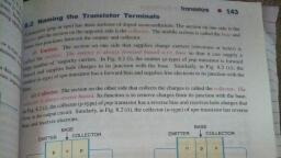
BASIC ELECTRICAL AND ELECTRONICS ENGINEERING, , The transistor was invented by a team of three scientists at Bell Laboratories, USA in 1947., Transistor is another important semiconductor device; it is equivalent to old three, electrode vacuum tube device that is „Triode‟., A transistor is basically consists of two words, transfer of resistor i.e. “Transistor”, (Transfer + Resistor Transistor)., Transistor working is more complex than diode but it is commonly observed in every port, of circuits in modern equipments., The most important feature of transistor is their ability of amplifying the weak signals, fast, switching action in other mode of its operation., Normally transistor is used as an amplifier but in digital or computer field it is used as, switch., There are two basic types of transistors:, 1. Bipolar junction transistor (BJT)., 2. Field-effect transistor (FET)., The bipolar junction transistor is used in two broad areas of electronics:, 1. As a linear amplifier to boost an electrical signal and, 2. As an electronic switch., Bipolar Junction Transistor (BJT):, 1. Bipolar transistor is similar to that of junction diode but one more junction is included., 2. Transistor is three terminal semiconductor device. (The three terminals are Emitter, Base,, and Collector)., 3. Basically, the bipolar junction transistor consists of two P-N junctions connected back-toback in the same structure of semiconductor material., 4. The transistor has two PN junctions., i., One junction is between the emitter and base is called as „Emitter-Base Junction‟, or „Emitter junction’., ii., The other junction is between the base and collector is called as „Collector-Base, Junction’ or ‘Collector junction’., 5. The transistor known as bipolar because both holes & electrons take part in the current, flow through device., 6. The bipolar junction transistor is simply a sandwich of one type of semiconductor material, between two layers of the other type., 7. There are two types of bipolar junction transistor:, i. NPN transistor: N-type material sandwiched between two layers of P-type material., ii. PNP transistor: P-type material sandwiched between two layers of N-type material., , Figure: (a) PNP schematic symbol, (b) physical layout (c) NPN symbol, (d) layout., 8. PNP Transistor:
Page 36 :
BASIC ELECTRICAL AND ELECTRONICS ENGINEERING, , For a NPN transistor, arrowhead points in the direction of conventional emitter, current flow from emitter to base. (from N to P region). For a PNP transistor, arrowhead, points from emitter to base meaning that emitter is +ve with respect to base., 9. NPN transistor:, The arrowhead points in the direction of conventional emitter current (from P to N, region.). For NPN transistor, it points from base emitter meaning that base is positive with, respect of emitter., , 10. Transistor has three terminals & three regions, taking NPN transistor into consideration, Emitter, Base, , : It is more heavily doped; its job is to emit the electrons into the base., : It is very lightly doped & it is thin ( 10 6 m) region as compare to either, emitter or collector, it passes most of the electrons towards collector., Collector : Since it collects the electrons from emitter and passing through the base,, its name is collector its doping level is medium between emitter & base. It, is a largest region., 11. Since emitter & collector made up to same semiconductor material, it cannot be, interchanged because of their difference in doping level., , Transistor Cutoff and Saturation Regions:
Page 37 :
BASIC ELECTRICAL AND ELECTRONICS ENGINEERING, , Region of Operation, Active Region, Saturation Region, Cutoff Region, , Emitter-Base Junction, Forward, Forward, Reverse, , Collector-Base Junction, Reverse, Forward, Reverse, , NPN Transistor Configuration:, When transistor is formed electrons across the junction produces two depletion layers., The width of potential barrier at base-emitter and base-collector is different, it is less near to, emitter base and more near collector because of difference in doping level as shown., , Figure: Biasing of NPN transistor and circuit symbol, 1. To make current flow through transistor easier it must be properly biased., 2. Hence we must have two DC voltage source or batteries, to apply bias across Emitter-Base, & Base-Collector junction., 3. Now we can bias these two junctions in three ways as,, a) FF bias, : Both junctions are forward bias (saturation region)., b) FR bias, : One forward and other reversed bias (Active region)., c) RR bias, : Both junctions are reversed bias (Cut-off region)., 4. In FF bias both junctions are forward bias. Hence large current flows through transistor as, it flows through forward bias diode simply behaves as low resistance; but there is no, control on this current., Similarly in third case RR bias, current through transistor is negligible it behaves, as a nonconducting or high resistance. Therefore transistor never be used in these two bias, system., 5. However, second method of biasing, one of the junction is forward bias & other is reversed, bias, in this condition transistor behaves as an electronic control device., 6. In practice (E-B) emitter-base junction is always forward biased & (B-C) base-collector, junction is reversed biased., 7. We know that the transistor is a "CURRENT" operated device and that a large current, ( I C ) flows freely through the device between the collector and the emitter terminals., However, this only happens when a small biasing current ( I B ) is flowing into the base, terminal of the transistor thus allowing the base to act as a sort of current control input.
Page 38 :
BASIC ELECTRICAL AND ELECTRONICS ENGINEERING, , 8. The ratio of these two currents ( I C / I B ) is called the DC Current Gain of the device and, is given the symbol of hfe or now a day‟s Beta, (β). Beta has no units as it is a ratio., 9. Also, the current gain from the emitter to the collector terminal, I C / I E , is called Alpha,, (α), and is a function of the transistor itself., 10. As the emitter current I E is the product of a very small base current to a very large, collector current the value of this parameter α is very close to unity, and for a typical lowpower signal transistor this value ranges from about 0.950 to 0.999., , Figure: Biasing of NPN transistor, Observe the battery connections a single cell low voltage is connected but forward bias is, applied across E-B junction and high voltage is applied across B-C junction but in reverse bias., Now observe emitter is connected to negative terminal. It repells electrons towards the junction,, they enter in the base region but base is P-region and it is lightly doped. It has very less number, of electrons attracted by +ve terminal of VBE battery or holes are passed by this positive terminal, into the base. Rests of the electrons are attracted by positive terminal of battery Vcc., Battery voltage Vcc is comparatively high voltage, therefore almost all electrons are, attracted by collector terminal only few are passed base to battery. To understand this, let us take, an illustration with 100 electrons emitted by emitter., Transistor Currents:, The three primary currents which flow in a properly-biased transistor are I E , I B and I C ., The total current flowing into the transistor must be equal to the total current flowing out, of it. Hence, the emitter current I E is equal to the sum of the collector ( I C ) and base current, ( I B ). That is,, , IE IB IC, The currents directions are positive directions. The total collector current IC is made up of, two components., I, 1. The fraction of emitter (electron) current which reaches the collector ( α, dc E ), 2. The normal reverse leakage current I CO .
Page 39 :
BASIC ELECTRICAL AND ELECTRONICS ENGINEERING, , ‘ α dc ’ is known as large signal current gain or dc alpha. It is always positive. Since, collector current is almost equal to the I E therefore α, , I, dc E varies from 0.9 to 0.98. Usually, the, reverse leakage current is very small compared to the total collector current., In figure are shown the directions of flow as well as relative magnitudes of these currents, for a PNP transistor connected in the common-base mode., IE IB IC, It means that a small part (about 1-2%) of emitter goes to supply base current and the, remaining major part (98-99%) goes to supply collector current., Moreover, I E flows into the transistor whereas both I B and I C flow out of it., , Figure: Idea of I B , I C , I E, We have studied, large no. of electrons are emitted (repelled) by emitter (Suppose 100, electrons) towards base, two electrons are lossed in recombination with holes of P region base., Therefore two electrons are generated in P type material those are collected by base, it is denoted, by base current “ I B ”. The majority of 98 electrons are collected by collector and those are, collected by positive terminal of Vcc and it is indicated by “Ic”., Thus we can say,, Emitter current = Base Current + Collector Current, (100 electrons) = (2 electrons) + (98 electrons), , IE IB IC, This equation says that emitter current is the sum of base current and collector current., Figure shows the direction of current as conventional current opposite to electron flow.
Page 40 :
BASIC ELECTRICAL AND ELECTRONICS ENGINEERING, , Above figure shows the flow of currents in the same transistor when connected in the, common-emitter mode. It is seen that,, , IE IB IC ., By normal convention, currents flowing into a transistor are taken as +ve whereas those, flowing out of it are taken as –Ve. Hence, I E is +Ve whereas both I B and I C are –Ve., Applying Kirchhoff‟s Current Law, we have,, , I E I B (I C ) 0, , or, , IE IB IC 0, , or, , IE IB IC, , Alpha and Beta of transistor:, As we have in last topic the emitter current flows two paths only 2 to 5% current flows, through base and 98 to 95 % through collector. Since the emitter current is the input current, and, the collector current is the output current, the current gain is denoted by „α‟ and it is given by,, I, Output Current, α C, , IE, Input Current, The „α‟ of a transistor is a measure of the quality of a transistor, higher the value of α,, better the transistor in the sense that collector current more closely equals the emitter current. Its, value ranges from 0.95 to 0.999., For example out of 100 electrons 98 electrons flows through collector as we have, considered the current gain is calculated as, 98, , 0.98, 100, Thus current gain is always less than unity but approximately I C = I E almost collector, current is equal to emitter current, because base current is very small. This current gain is, applicable in common base configuration. While in common emitter configuration, base current, is the input current. This is expressed in terms of „β‟ and it is known as “Current Amplification, Factor”., I, C, IE, Relation Between α and β:
Page 41 :
BASIC ELECTRICAL AND ELECTRONICS ENGINEERING, , The relation between α and β can be obtained as,, , But,, , Now, , IE IC IB, , ……………..………… (I), , IC, α, IE, IC α IE, IE IB IC, IB IE IC, , ……………………….. (II), , IB IE α IE, I B I E (1 α ), , ……………………….. (III), , Now „β‟ is defined as,, , IC, IB, α IE, β, I E (1 α ), β, , β, , α, (1 α ), , &, , (Substituting II and III), , α, , β, (1 β ), , Three Configurations of Transistor:, An amplifier is one of the most common circuits of transistor. These configurations of, transistor are possible depending on input and output voltage taken across which electrode and, the name to the configuration is given according to the electrode which is common to both input, and output., There are three configurations of transistor, Common base configuration - has Voltage Gain but no Current Gain., Common Emitter configuration - has both Current and Voltage Gain., Common collector configuration - has Current Gain but no Voltage Gain., , Common Base configuration (PNP Transistor Configuration):
Page 42 :
BASIC ELECTRICAL AND ELECTRONICS ENGINEERING, , Figure: Working of PNP transistor, The action of PNP transistor is quite similar to that NPN transistor. The difference, here is the polarities of biasing batteries which are reverse to that of NPN transistor;, observe figure flow of current is due to holes which are majority carriers. The direction of, current is shown by figure., , Same current flows through base, emitter and collector that is,, IE IB IC, , IC β IB, , IB , , IC, β, , Also this type of bipolar transistor configuration has a high ratio of output to input, resistance or more importantly "load" resistance ( RL ) to "input" resistance ( Rin ) giving it, a value of "Resistance Gain"., Common Emitter Configuration:, In this type of configuration, the current flowing out of the transistor must be equal, to the currents flowing into the transistor as the emitter current is given as, I E I C I B ., Also, as the load resistance ( R L ) is connected in series with the collector, the, Current gain of the Common Emitter Transistor Amplifier is quite large as it is the ratio of, I C / I B and is given the symbol of Beta, (β). Since the relationship between these three, currents is determined by the transistor itself, any small change in the base current will, result in a large change in the collector current. Then, small changes in base current will, thus control the current in the Emitter/Collector circuit.
Page 43 :
BASIC ELECTRICAL AND ELECTRONICS ENGINEERING, , By combining the expressions for both Alpha, α and Beta, β the mathematical, relationship between these parameters and therefore the current gain of the amplifier can, be given as:, , IE IC IB, , IC, IE, β, α, β 1, α, , &, , β, , β, , IC, IB, , α, 1 α, , Where: " I C " is the current flowing into the collector terminal, " I B " is the current flowing, into the base terminal and " I E " is the current flowing out of the emitter terminal., Then to summaries, this type of bipolar transistor configuration has a greater input, impedance, Current and Power gain than that of the common Base configuration but its Voltage, gain is much lower. The common emitter is an inverting amplifier circuit resulting in the output, signal being 180o out of phase with the input voltage signal., Common Collector Configuration:, , , , In this configuration collector terminal is connected as a common terminal., The input is applied between the base and collector terminals. The output is taken, between the emitter and collector terminals, , Transistor Characteristics:
Page 44 :
BASIC ELECTRICAL AND ELECTRONICS ENGINEERING, , The static characteristics for Bipolar Transistor amplifiers can be divided into the, following main groups., - IE ÷ VEB, Input Characteristics:- Common Base, Common Emitter - IB ÷ VBE, Output Characteristics:- Common Base, - IC ÷ VC, Common Emitter - IC ÷ VC, Transfer Characteristics:- Common Base, - IE ÷ IC, Common Emitter - IB ÷ IC, , Common Base Configurations characteristics:, Input Characteristics, , The output (CB) voltage is maintained, constant and the input voltage (EB) is set at, several convenient levels. For each level of, input voltage, the input current IE is, recorded., IE is then plotted versus VEB to give the, common-base input characteristics., , Output Characteristics, , The emitter current IE is held constant at each, of several fixed levels. For each fixed value of, IE , the output voltage VCB is adjusted in, convenient steps and the corresponding levels, of collector current IC are recorded, .For each fixed value of IE, IC is almost equal to, IE and appears to remain constant when VCB is, increased., , Common Emitter Configuration:, Input Characteristics, , Output Characteristics, , The output voltage VCE is maintained The Base current IB is held constant at each, constant and the input voltage VBE is set at, of several fixed levels. For each fixed value of, several convenient levels.For each level of, IB , the output voltage VCE is adjusted in, input voltage, the input current IB is, convenient steps and the corresponding levels, recorded., of collector current IC are recorded, IB is then plotted versus VBE to give the For each fixed value of IB, IC level is, common-base input characteristics., Recorded at each VCE step. For each IB level,, IC is plotted versus VCE to give a family of
Page 45 :
BASIC ELECTRICAL AND ELECTRONICS ENGINEERING, , characteristics., Graph:, , Graph:, , Common Collector configuration Characteristics:, Input Characteristics, , Output Characteristics, , The common-collector input characteristics, are quite different from either common base, or common-emitter input characteristics., The difference is due to the fact that the input, voltage (VBC) is largely determined by (VEC), level., VEC = VEB + VBC, VEB = VEC - VBC, , The operation is much similar to that of C-E, configuration. When the base current is ICO,, the emitter current will be zero and, consequently no current will flow in the load., When the base current is increased, the, transistor passes through active region and, eventually reaches saturation. Under the, saturation conditions all the supply voltage,, except for a very small drop across the, transistor will appear across the load resistor., , Comparison of Different Configurations:, Parameters, , Common Base, , Common Emitter, , Common Collector
Page 46 :
BASIC ELECTRICAL AND ELECTRONICS ENGINEERING, , I/p-O/p Phase, relationship, Voltage Gain, , 0°, , 180°, , 0°, , High (100), , Low (almost unity), , Current Gain, , Low (almost unity), , Power Gain, Input Resistance, Output Resistance, , Low, Low (100Ω), High (400KΩ), , Medium, Medium ( in the order, of hundreds), High, Medium (700Ω), Medium (45 KΩ), , High, Medium, High (MΩ), Low (Ω), , Application of transistor:, CE Amplifier (Transistor as an amplifier):, 1) In electronics, a common-emitter amplifier is one of three basic single-stage bipolarjunction-transistor(BJT) amplifier topologies, typically used as a voltage amplifier., 2) In this circuit the base terminal of the transistor serves as the input, the collector is the, output, and the emitter is common to both (for example, it may be tied to ground, reference or a power supply rail), hence its name., 3) Amplification is the process of linearly increasing the amplitude of an electrical signal and, is one of the major properties of a transistor., 4) As you learned, a BJT exhibits current gain (called b). When a BJT is biased in the active, (or linear) region, as previously described, the BE junction has a low resistance due to, forward bias and the BC junction has a high resistance due to reverse bias., , Figure: CE Transistor Amplifier, 5) When we speak in a microphone, sound is converted into electrical signal that is known as, an audio frequency signal. These signals are transmitted with radio frequency which is, high frequency signals. Similarly the signal generated by record player and tape-recorder,, all these signals are weak signals. These signals are amplified by a circuit called as an, amplifier., “The action of amplifier is the process of increasing the amplitude of input signal, with the help of DC supply”
Page 47 :
BASIC ELECTRICAL AND ELECTRONICS ENGINEERING, , Most common configuration which is used an amplifier is common emitter (CE), configuration. Figure shows a CE amplifier circuit. The input signal is applied across base, and ground of the transistor. The output signal appears across collector to ground., 6) There are two resistors in the circuit, R 1 is connected to base, it is selected to limit the, base current. Here R 1 is called as base bias resistor. Other resistor is R L (load resistor), which is required to develop output voltage across collector to emitter ( VCE ). If there is, collector resistor then collector voltage will be DC (+Vcc)., , Transistor (BJT) as Switch:, 1) Figure illustrates the basic operation of a BJT as a switching device., , Figure: Switching action of an ideal transistor, 2) In part (a), the transistor is in the cutoff region because the base-emitter junction is not, forward-biased.
Page 48 :
BASIC ELECTRICAL AND ELECTRONICS ENGINEERING, , 3) In this condition, there is, ideally, an open between collector and emitter, as indicated by, the switch equivalent., 4) In part (b), the transistor is in the saturation region because the base emitter junction and, the base-collector junction are forward-biased and the base current is made large enough, to cause the collector current to reach its saturation value., 5) In this condition, there is, ideally, a short between collector and emitter, as indicated by, the switch equivalent. Actually, a small voltage drop across the transistor of up to a few, tenths of a volt normally occurs, which is the saturation voltage, VCE (sat)., , , Conditions in Cutoff:, A transistor is in the cutoff region when the base-emitter junction is not forwardbiased. Neglecting leakage current, all of the currents are zero, and VCE is equal to VCC ., , VCE (Cut-off) = VCC, , , Conditions in saturation:, When the base-emitter junction is forward-biased and there is enough base current, to produce a maximum collector current, the transistor is saturated. The formula for, collector saturation current is, VCC VCE (sat), I C( sat) , RC, Since VCE (sat) is very small compared to VCC , it can usually be neglected., The minimum value of base current needed to produce saturation is, I C (sat), IB , β DC, Normally, I B should be significantly greater than I B (min) to ensure that the, transistor is saturated., , Photo Transistor:, , Figure: Symbol of photo transistor, 1) The phototransistor is similar to a regular BJT except that the base current is produced, and controlled by light instead of a voltage source., 2) The phototransistor effectively converts variations in light energy to an electrical signal., 3) The phototransistor is a transistor in which base current is produced when light strikes the, photosensitive semiconductor base region., 4) The collector-base p-n junction is exposed to incident light through a lens opening in the, transistor package., 5) When there is no incident light, there is only a small thermally generated collector to, emitter leakage current, I CEO ; that is called the dark current and is typically in the nA
Page 49 :
BASIC ELECTRICAL AND ELECTRONICS ENGINEERING, , range. When light strikes the collector-base p-n junction, a base current I , is produced, that is directly proportional to the light intensity. This action produces a collector current, that increases with I . Except for the way base current is generated, the phototransistor, behaves as a conventional BJT. In many cases, there is no electrical connection to the, base., 6) The relationship between the collector current and the light-generated base current in a, phototransistor is,, , I C β DC I , 7) The schematic symbol and some typical phototransistor are shown in figure. Since the, actual photo generation of base current occurs in the collector-base region, the larger the, physical area of this region, the more base current is generated. This, a typical, phototransistor is designed to offer a large area to the incident light., , Figure: Typical phototransistor structure, ---------------------------------------------------------------------------------------------------------------, , Assignment No. 2
Page 50 :
BASIC ELECTRICAL AND ELECTRONICS ENGINEERING, , 1. Explain reverse bias characteristics of PN junction diode., 2. Explain half wave rectifier and full wave rectifier with necessary diagrams., 3. What is an amplifier? How does a transistor work as an amplifier? Explain the field of, application of amplifiers., 4. Identify the mostly used transistor configuration out of CB, CE, CC. Explain the same with, circuit diagram and operation., 5. Explain the working of bridge rectifier. Define the terms:, a. Rectification efficiency, b. TUF, Compare half wave rectifier, full wave rectifier and bridge rectifier., 6. Compare different transistor configurations on the basis of input resistance, output resistance,, voltage gain and applications of each configuration., 7. Explain the operation of Zener diode voltage regulator circuit., 8. Draw circuit diagram of VI characteristics of PN junction diode. Explain VI characteristics of, diode with the help of diode equation., 9. Explain the operation of full wave rectifier with center tap transformer. Draw input and output, waveforms., 10. What are impurities added to intrinsic semiconductors to get P type and N type extrinsic, semiconductor? Explain biasing of diode., 11. Explain biasing of transistor and CE, CB, CC configuration of transistor. Also compare, between different configurations., 12. Explain the working of transistor in CE configurations. Explain the input and output, characteristics of CE configuration., 13. Explain in brief photo diode and photo transistor. Also compare them., 14. Why filters are required? Draw the circuit diagram of full wave rectifier using two diodes and, capacitor filter. Also explain its working and draw necessary diagrams., 15. What is need of filter? Explain capacitor filter.