Page 1 :
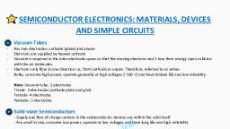
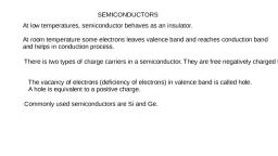
SEMICONDUTOR CHAPTER, 1) INRINSIC SEMICONDUTOR:, 1., , The pure semiconductors are considering as intrinsic semiconductors, because in these, semiconductor does not have any kind of impurities., , 2., , These behave as an insulator at 0K (at low temperature) and at higher temperature these, behaves as conductor., Ex: Si, Ge (4th group elements), , 3., , The Fermi level exists exactly at midway of the energy gap (at half way distance from, conduction and valance bands), , 4., , In an Intrinsic Semiconductors the no. of e - presented conduction band (n) is equivalent to, the no of holes presented in an valance band (p), [n=p], , Carrier concentration and Fermi level equation of intrinsic semiconductor:, , Derive the carrier concentration equation, Derive the Fermi level equation
Page 2 :
2) EXTRINSIC SEMICONDUTOR:, 1. A semiconductor which has doping with impurity either the donor impurities or the acceptor, impurities such as 3rd group or 5th group elements. Is known as extrinsic semiconductor., 2. The addition of impurity increases the carrier concentration and hence the conductivity of the, conductor increases., 3. Based on the impurities, the extrinsic semiconductors are classified into two types, a., , N-type semiconductor, , b., , P-type semiconductor, , 2.1) N TYPE SEMICONDUCTOR:, , 1. When any one such impurity i.e. pentavalent (+5) elements such as, P, As, Sb ……. Have, five electrons in their outermost orbits is added to intrinsic semiconductor., 2. Four electrons are engaged in with four neighboring pure semiconductor atoms, the fifth, electron is weakly bound to the parent atom., 3. The energy level of the fifth electron is called donor energy level, this donor energy level, close to the bottom of the conduction band., 4. Even for lesser thermal energy this fifth electron is release, the parent atom +Ve ionised., During this process hole is generated in donor level., 5. Since these pentavalent elements donate –Ve charges, they are called “N-type impurities”, and the semiconductors doped with pentavalent impurities are called “N-type, semiconductors”.
Page 3 :
6. Most of the donor level electrons are excited into the conduction band at room and become, the “majority charge carriers”., 7. If the thermal energy is sufficiently high (increase temperature), in addition to the ionization, of donor impurity atoms, breaking of covalent bond may also occur these by giving rise to, generation of electron-hole pair., 8. Hence in N-type semiconductor, “Electrons are majority carriers” & “Holes are minority carriers”., Carrier Concentration equation of N-type semiconductor:, , Derive the carrier concentration equation with Fermi level representation., , Variation of Fermi level with Temperature:, (Variation of Fermi level with donor concentration):, , 1. Temperature increases the Fermi level (EF) increases slightly. As that temperature is, increased, more and more donor atoms are get ionized., 2. For a particular temperature all the donor atoms are ionized. Further increase in temperature, results in generation of electron-hole pairs to breaking of covalent bonds and the material, tends to behave in intrinsic manner., 3. The Fermi level gradually moves towards the intrinsic Fermi level (Ei) as shown in figure.
Page 4 :
2.2) P TYPE SEMICONDUCTOR:, , 1. When any one such impurity i.e. trivalent (+3) elements such as Aluminum (Al), Gallium, (Ga), Indium (In) ……., have three electrons in their outermost orbits is added to intrinsic, semiconductor., 2. Three electrons are engaged in with three neighboring pure semiconductor atoms (Ge, atom)., 3. Indium (In) needs one more electron to complete its bond. This electron may be supplied, by Ge atom. Then creating a vacant electron site or hole on the semiconductor atom., 4. The energy level of the electron site or hole is called accepter energy level, this accepter, energy level lies just above to the valance band., 5. These type of trivalent impurities are called acceptor impurities and the semiconductors, doped with acceptor impurities are called P-type semiconductors., 6. At low temperatures these acceptor atoms get ionized taking electrons from valance band, and created the hole more in valance band for conduction., 7. If temperature is sufficiently high (increase temperature), in addition to above process get, ionized atoms and more no of electrons transfer from valance band to accepter energy, level, due to breaking of covalent bond may also occur these by giving rise to generation, of electron-hole pair., 8. Hence in P-type semiconductor, “Holes are majority carriers” & “Electrons are minority carriers”.
Page 5 :
Carrier Concentration equation of P-type semiconductor:, , Derive the carrier concentration equation with Fermi level representation., , Variation of Fermi level with Temperature:, (Variation of Fermi level with acceptor concentration):, , 4. Temperature increases the Fermi level (EF) decreases slightly. As that temperature is, increased, more and more acceptor atoms are get ionized., 5. For a particular temperature all the acceptor atoms are ionized. Further increase in, temperature results in generation of electron-hole pairs to breaking of covalent bonds and the, material tends to behave in intrinsic manner., 6. The Fermi level gradually moves towards the intrinsic Fermi level (Ei) as shown in figure.
Page 6 :
3. P-N Junction diode:, 3.1) Formation of PN junction diode (unbiased PN junction, diode (OR) Open circuit PN junction diode), , 1. In a piece of semiconductor material, if one half is doped by P-type impurity and the other, half is doped by N-type impurity, a P-N junction is formed, it is called “P-N Junction”., 2. In P-N junction, P-type region has excess of holes, N-type region has excess of electrons,, Which are loosely held by ionized acceptors and donors, hence these are free to move at, normal temperature., 3. At the junction, some of the electrons of N-region diffuse into P-region; they recombine with, equal number of holes., 4. Similarly, some of the holes of P-region diffuse into N-region; they recombine with equal, number of electrons., 5. Which are diffuse and recombined are called migrating electrons & migrating holes., 6. The electron-hole recombination process makes donor atoms immobile positive (+Ve) ions in, the N-region, the acceptor atoms immobile negative (-Ve) ions in the P-region near junction., 7. Due to presence of these +Ve and -Ve charges developed near junction, a negative (-Ve), potential is built up in the P-region and positive (+Ve) potential is built up in the N-region to, near the junction.
Page 7 :
8. The difference in potential in two regions is known as the built-in potential (or) potential, barrier (VB) and the corresponding electric field is called the barrier field., 9. Thus the region in which the barrier field exists is deflected of charge carriers and is known, as “depletion region” or “space charge region” or charged free region” or “potential, barrier”., 10. The potential barrier (VB) is of the order of “0.1 to 0.3 Volt”., 11. The difference in electron energies in the two regions is known as the barrier energy,, it is EB = eVB., 12. This energy is required by an electron to move from N-region to P-region and the equal, amount of energy is required by a hole to cross the depletion layer in the opposite direction., 13. Hence, “Majority charge carriers “produced the “diffusion current” and “Minority, charge carriers” produced the “drift current”, these both are in equal and opposite, direction., 14. This phenomenon is called “Unbiased P-N Junction diode or Open circuit P-N Junction”., 3.2), , P-N JUNCTION IN FORWARD BIAS:, , 1. The +Ve terminal of a battery is connected to P-type semiconductor while the –Ve terminal, of a battery is connected to N-type semiconductor as shown in fig., is known as “forward, bias”., 2. When an external voltage is applied to P-N Junction in such a direction, it cancels the, potential barrier and permits the current flow is called as “forward bias”.
Page 8 :
3. Due to applied external voltage the potential barrier is reduced and establishes an electric, field opposite to the potential barrier., 4. Required forward voltage to completely eliminate the potential barrier is, for Ge = 0.3Volts, and for Si = 0.7 Volts., 5. When potential barrier is eliminated by the forward voltage across junction the “resistance”, becomes almost “zero”., 6. In the forward bias, the holes from P-type semiconductor are repelled by the +Ve battery, terminal towards the junction. Simultaneously, the electrons in N-type semiconductor are, repelled by –Ve battery terminal towards junction., 7. When an sufficient energy given to these carriers, to overcome the potential barrier at the, junction, develop the constant movement of electrons towards +Ve terminal and the holes, towards the –Ve terminal across the potential barrier., 8. Hence, in forward bias produces a low resistance path is established and high Forward, current., 3.3), , P-N JUNCTION IN REVERSE BIAS:, , 1. The +Ve terminal of the battery is connected to N-type semiconductor and –ve terminal to Ptype semiconductor as shown in fig., is known as “Reverse bias”., 2. When an external voltage is applied to P-N Junction, it increases the “potential barrier” then, it is called as “Reverse bias”., 3. Due to applied reverse voltage, the potential barrier width is increased and establishes an, electric field in the same direction of potential barrier.
Page 9 :
4. The potential barrier prevents the flow of charge carriers across the junction; hence high, resistance path is established., 5. When the junction is reversed biased the electrons in N-type semiconductor and holes in Ptype semiconductor are attracted away from the junction., 6. Since, there is no recombination of electrons hole pairs no current flows in the circuits., , From the above forward bias and reverse bias discussion., 1. When a P-N junction is forward bias, it has a low resistance path and hence current flows, in the circuit., 2. When a P-N junction is reverse bias, it has high resistance path and no current flows in the, circuit., 3. Thus P-N junction diode is one-way device which offers a low resistance when forward, biased and behaves like insulator when reverse biased., 4. Thus it can be used as a rectifier i.e. for converting alternating current (a.c.) into direct, current (d.c.), 3.3) I-V CHARACTERISTIC OF P-N JUNCTION DIODE:, , Fig: 1, Figure 1 shows the circuit arrangement for drawing the Volt – Ampere characteristics of a P-N, junction diode., Figure 2 shows the Plot graph between Volt – current & Figure 3 shows diode symbol.
Page 10 :
1. When no external voltage is applied the circuit current is Zero it is said to be, “UNBIASED CIRCUIT”, 2. The characteristics are studied under the following biases, Forward biased circuit, Reverse biased circuit, Forward biased circuit:, a) When “+Ve” terminal of the battery is connected to P-type and “-Ve” terminal of battery is, connected to N-type, the junction is said to be “Forward bias”., b) When the voltage applied about 0.3Volt for Ge and 0.7Volt for Si, the potential barrier is, altogether eliminated and current starts flowing. This voltage is known as “Threshold, voltage” or “Cut-in voltage” or “Knee voltage”., c) When the applied voltage exceeds the above values, the junction resistance becomes almost, zero and it established “low resistance path”., d) Hence, for small increases of applied voltage, we observe large increases in circuit current., So, it is called “forward bias circuit” and the current is called “forward current”., e) The forward current measured in milli Aamper (mA) and it is found to increases linearly, with the applied voltage., Reversed biased circuit:, a) When reverse biased, a little reverse current (micro ampere (μA)) pass in the circuit., b) Even for large applied voltage, there is negligible increase in reverse current., c) When the applied reverse voltage is high enough to break the covalent bonds, the current, rises suddenly in the reverse direction., d) The breakdown reverse bias is called “breakdown voltage” or “Zener voltage”
Page 11 :
3.4), , ENERGY LEVEL DIAGRAM OF P-N JUNCTION DIODE:, , Ec – Energy level in conduction band, Ef – Fermi level position, , Ev – Energy level in valance band, , Ecp – Conduction band energy state in p type semiconductor, Efp – Fermi level position in p type semiconductor, Evp – Valance band energy state in p type semiconductor, Ecn – Conduction band energy state in n type semiconductor, Efn – Fermi level position in n type semiconductor, Evn – Valance band energy state in n type semiconductor., Built in potential in N-region = Vn, Built in potential in P-region = Vp, Built in potential across potential barrier = VB = Vn-Vp., The energy required for migrating the electron from n-region to p-region or hole, migrating from p-region to n-region is, , EB = eVB = e (Vn-Vp), EB = Evp – Evn = Ecp – Een = eVB
Page 12 :
1. At unbiased condition applied voltage V = 0, and the Fermi level at midway to, conduction band and valance band., Hence, VB = Vn - Vp, 2. In forward bias applied external voltage V= Vf across the depletion region. The VB acts, from N to P and the Fermi level is near to conduction band in n-region and near to, valance band in p-region, So, the potential barrier is decreases,, Hence, VB = VB – Vf, 3. In reverse bias applied external voltage V= Vr across the depletion region. The V B acts, along VB and the Fermi level is away to conduction band in n-region and away to, valance band in p-region, So, the potential barrier is increases,, Hence, VB = VB – Vr
Page 13 :
3.4) ZENER DIODE:, 1. “Zener diode” is a reversed biased Heavily-doped Si or Ge P-n junction diode which is, operated in the “breakdown region”., 2. “Si” is preferred in comparison to “Ge” due to higher temperature and current capability., 3., , It is observed that as the reverse voltage applied to p-n junction is increased from zero, the, current remains very small over a long range and increases very slightly with increasing bias., , 4. But when the reverse bias is made very high, the covalent bonds near the junction breaks, down. Now the reverse current increases to a large value., The corresponding voltage is called “break down voltage” or, “zener voltage”., 5., , In this region the voltage across the diode remains constant over a large, range of current”., , 6. Hence the zener diode may be used to stabilize voltage at a predetermined, value., 7. Zener diode, reverse bias is only applied and operated in Break-down region., , There are two mechanisms of the breakdown., 1. Zener breakdown: It takes place in very thin junction. i.e when both sides of junctions are, very heavily doped and consequently the depletion layer is narrow., 2. When a small reverse bias voltage is applied, a very strong electric field (above 107 V/m) is, setup across the thin depletion layer. This field is enough to break the covalent bonds., 3. Zener current is independent of the applied voltage and depends only on the external, resistance.
Page 14 :
4. Avalanche breakdown: when both sides of junctions are lightly doped and consequently the, depletion layer is large., 5., , In this case, the electric field across the depletion layer is not so strong to produce zener, breakdown., , 6., , Hence, the minority carriers accelerated by the filed collide with the semiconductor atoms, in the depletion region., , 7., , Due to collision with valance electrons, covalent bonds are broken and electronpairs are generated., , 8., , These new carriers so produced acquired energy from applied potential and in turn, produce additional carriers., , 9., , This forms a cumulative process called as avalanche multiplication. The breakdown is, called avalanche breakdown as shown in fig., , 10., , hole, , This breakdown occurs at higher reverse voltages., , 11. “At reverse voltages < 6V for Zener breakdown, At reverse voltages > 8V for Avalanche breakdown”, 12. The zener diode is most suited for voltage regulator, , Zener diode as voltage stabilizer:, , The zener diode is connected to a battery “B” through Resistor “R”. The battery “B”, Reverse-biased the zener diode., The load RL is connected across the terminals of diode., the value of R is selected in such a way that in the absence of load RL maximum safe current, flows in the diode as zener diode., Now, consider that the load is connected across the diode, the load draws a current. The, current through the diode falls by the same amount but the voltage drop across the resistance, R. almost remains constant., In this way variation in in load current hardly affected the voltage V supplied to it.
Page 15 :
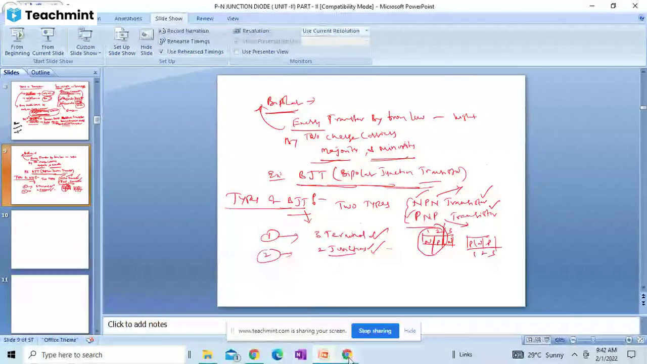
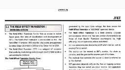
4) BI-POLAR JUNCTION TRANSISTOR (BJT):, , In electronic devices most essistinential device is BJT., Most essential in-radiant in most of the electrons Amplifier, Oscillator, and our day to day, life used digital computers and also in IC (Integrated circuit)., For amplification purpose we are passing signal through small resistance i.e., transferring, signal from “low resistance” to “high resistance” area, hence it is called “transistor”, Depends on carrying a “charge or current” they are two type of transistors., UNI-POLAR –Current is flowing because of only “majority charge carriers, Ex: JFET (Junction Field Effect Transistor), MOSFET (Metal Oxide Semiconductor FET)., BI-POLAR – Current is flowing because of both “Majority charge carriers, & Minority charge carriers”, Ex: BJT (Bipolar Junction Transistor), , 4.1) Bipolar Junction Transistor (BJT) Construction:, It is an three (3) terminal or two (2) junction diode, It is an three (3) layer device, By using P-type & N-type semiconductor, we construct two type, they are, i), NPN Transistor, ii) PNP Transistor, , N-P-N TRANSISTOR CONSTRUCTION:
Page 16 :
P-N-P TRANSISTOR CONSTRUCTION:, , 1) When a layer of P type material is placed between two layer of N type material, is known, as N-P-N transistor, 2) When a layer of N type material is placed between two layer of P type material, is known, as P-N-P transistor, 3) Transistors are made either from “Si or Ge”., 4), , Emitter:, i), ii), iii), iv), , 5), , Base:, i), ii), , 6), , It is heavily doped and moderated area, It is made physically larger area than collector and small area than base region., It emits charge carriers either electrons or holes (majority charge carriers)., It provided so many no of electrons and holes for current conduction, because, both electrons and holes will be participated in the current conductions., , It is very lightly doped and small area (10-6 m), Less recombination – more current, More recombination – less current, , Collector:, i), ii), iii), , It is moderate doping, It should collecting the charge carriers either electrons or holes which are from, emitter., It is made physically larger area than emitter and base region.
Page 17 :
OPERATION MODES IN BJT:, Mode of operations, , Emitter-Base-Junction, (EBJ), , Collector-Base-Junction, (CBJ), , Cut-off ( Switching purpose), , Reverse Bias, , Reverse Bias, , Active (Amplification purpose), , Forward Bias, , Reverse Bias, , Saturation (Switching purpose), , Forward Bias, , Forward Bias, , Reverse Active (Amplification, purpose), , Reverse Bias, , Forward Bias, , 4.2) OPERATION OF N-P-N TRANSISTOR:, , 1. In N-P-N transistor “emitter-base junction” as “forward bias” and “Collector – base, junction” as “reverse bias”., 2. The electrons of N-region (emitter) are repelled by the “–Ve” terminal of battery VEE, towards the base.
Page 18 :
3. The potential barrier at emitter junction is reduced as it is forward bias and hence the, electrons cross this junction and penetrate into P-region. This consistitute the emitter, current (IE)., 4. The width of the base region is very thin and it is lightly doped and hence only 2% to 5%, of the electrons recombine with the free holes of P-region. This consistitute the base, current (IB), 5. The remaining electrons (95% to 98%) are able to drift across the base and enter the, collector region., 6. They are received by the “+Ve” collector voltage VCC. They consistitute the collector, current (IC)., 7. At each electron reaches the collector electrode, a hole is emitted from the “+Ve”, terminal of battery and neutralized the electrons., 8. The liberated hole enter the “-Ve” terminal of battery VEE while the electron immediately, moves towards the emitter junction., 9. This process is repeated again and again continuously so long as the two junctions are, properly biased., 10. In N-P-N transistor, a) Current conduction within NPN transistor takes place by electron conduction, from emitter to collector., i.e. majority charge carriers in a NPN transistor are “electrons”. The, conduction in the external circuit is carriers out by “holes”., b) In operation of NPN transistor only the “electron current” plays an important, role., IE=IB+IC
Page 19 :
4.3) OPERATION OF P-N-P TRANSISTOR:, , 1. In P-N-P transistor “emitter-base junction” as “forward bias” and “Collector – base, junction” as “reverse bias”., 2. The holes of P-region (emitter) are repelled by the “+Ve” terminal of battery VEE towards, the base., 3. The potential barrier at emitter junction is reduced as it is forward bias and hence the, holes cross this junction and penetrate into N-region. This consistitute the emitter current, (IE)., 4. The width of the base region is very thin and it is lightly doped and hence only 2% to 5%, of the holes recombine with the free electrons of N-region. This consistitute the base, current (IB), it is very small., 5. The remaining electrons (95% to 98%) are able to drift across the base and enter the, collector region., 6. They are received by the “-Ve” collector voltage VCC. They consistitute the collector, current (IC)., 7. At each hole reaches the collector electrode, an electron is emitted from the “-Ve”, terminal of battery and neutralized the electrons., 8. The liberated electron enter the “+Ve” terminal of battery VEE while the holes, immediately moves towards the emitter junction.
Page 20 :
9. This process is repeated again and again continuously so long as the two junctions are, properly biased., 10. In P-N-P transistor, a) Current conduction within PNP transistor takes place by hole conduction from, emitter to collector., i.e. majority charge carriers in a PNP transistor are “holes”. The conduction in, the external circuit is carriers out by “electrons”., b) In operation of PNP transistor only the “hole current” plays an important role., IE=IB+IC