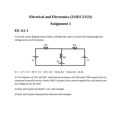
Page 1 :
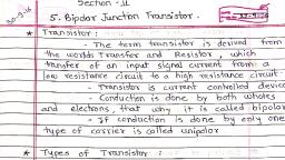
Transistor, • A transistor is a semiconductor device comes, with three terminals., • A transistor is termed as a trans resistor which, is used as switch or gate for electronic signals., • transistors are divided into two categories, called, • unipolar transistor Uses one charge carrier, bipolar transistor Uses two charge carrier, 08:59
Page 2 :
Application of Transistor, , •AMPLIFICATION, •SWITCH, , 08:59
Page 3 :
Transistor, • Bipolar Junction Transistor (BJT), – Bipolar, – Current controlled device, , • Field Effect Transistor (FET), – Unipolar, – Voltage controlled device, , 08:59
Page 4 :
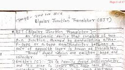
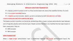
Bipolar Junction Transistor (BJT), • Introduced in 1948 by Shockley, BJT is an, electronic component mainly used for, switching and amplification purpose., • It is composed of three terminals called, emitter, base, and collector, denoted as E,, B and C respectively., • BJT comes in two types called NPN transistor, and PNP transistor., 08:59
Page 7 :
pnp and npn Transistor, Emitter, This has a moderate size and is heavily, doped as its main function is to supply a, number of majority carriers, i.e. either, electrons or holes., As this emits electrons, it is called as an, Emitter., This is simply indicated with the letter E., 08:59
Page 8 :
pnp and npn Transistor, Base, The middle material in the above figure is, the Base., This is thin and lightly doped., Its main function is to pass the majority, carriers from the emitter to the collector., This is indicated by the letter B, 08:59
Page 9 :
pnp and npn Transistor, Collector, Its name implies its function of collecting, the carriers., This is a bit larger in size than emitter and, base. It is moderately doped., This is indicated by the letter C., , 08:59
Page 13 :
npn transistor operation, • For normal operation of the transistor, the, • base-emitter (BE) forward biased, , • collector-base junction (CB) reverse, biased., • This is called as forward-reverse bias, configuration., 08:59
Page 14 :
08:59
Page 15 :
BJT voltages and currents:, • Terminal voltages for npn transistor:, , 08:59
Page 16 :
BJT voltages and currents:, • Terminal voltages for pnp transistor:, , 08:59
Page 17 :
Transistor currents:, , 08:59
Page 18 :
Transistor currents:, , 08:59
Page 19 :
Transistor currents:, , 08:59
Page 20 :
Transistor currents:, , 08:59
Page 21 :
Transistor currents:, , 08:59
Page 22 :
Regions of Operations of BJT, , 08:59
Page 23 :
Regions of Operations of BJT, , 08:59
Page 24 :
08:59
Page 25 :
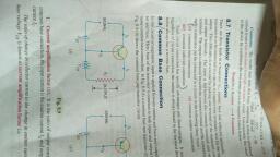
Three Basic Configurations of BJT, • 1. Common Base Configuration, • 2. Common Collector Configuration, • 3. Common Emitter Configuration, , 08:59
Page 26 :
Common Base Configuration, , 08:59
Page 27 :
Common Base Configuration, • Input Characteristics, , 08:59
Page 28 :
Common Base Configuration, • Output Characteristics, , 08:59
Page 29 :
Common Base Configuration, • Input Impedance, , Output Impedance, , 08:59
Page 30 :
Common Emitter Configuration, , 08:59
Page 31 :
Common Emitter Configuration, • Input Characteristics, , 08:59
Page 32 :
Common Emitter Configuration, • Output Characteristics, , 08:59
Page 33 :
Common Emitter Configuration, • Input Impedance, , Output Impedance, , 08:59
Page 34 :
Common Collector Configuration, , 08:59
Page 35 :
Common Collector Configuration, • Input Characteristics, , 08:59
Page 36 :
Common Collector Configuration, • Output Characteristics, , 08:59
Page 37 :
Common Collector Configuration, • Input Impedance, , Output Impedance, , 08:59