Notes of Class 12, Physics semiconductor (1).pdf - Study Material
Page 1 :
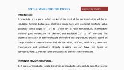
Semiconductor Electronics :, Materials, Devices and, Simple Circuits, Recap Notes, Classification of solids on the basis of, their conductivity : On the basis of the, relative values of electrical conductivity, (s) and resistivity (r = 1/s), the solids are, broadly classified as,, X Metals : Those solids which have high, conductivity and very low resistivity. The, value of conductivity for metals lies in, between 102 to 108 S m–1 and of resistivity, in between 10–2 to 10–8 W m., X Insulators : Those solids which have, low conductivity and high resistivity., The value of conductivity for insulators, lies between 10–11 to 10–19 S m–1 and of, resistivity between 1011 to 1019 W m., X Semiconductors : Those solids which, have, conductivity, and, resistivity, intermediate to metals and insulators. The, value of conductivity for semiconductors, lies in between 105 to 10–6 S m–1 and of, resistivity between 10–5 to 106 W m., Energy bands of solids or band theory of, solids, X Valence band : This band contains, valence electrons. This band may be, partially or completely filled with, electrons. This band is never empty., Electrons in this band do not contribute, to electric current., X Conduction band : In this band,, electrons are rarely present. This band is, either empty or partially filled. Electrons, in the conduction band are known as free, electrons. These electrons contribute to, the electric current., , X, , X, , X, , X, X, , Forbidden energy gap or forbidden, band : The energy gap between the, valence band and conduction band, is known as forbidden energy gap or, forbidden band. No electrons are present, in this gap. It is a measure of energy band, gap., The minimum energy required for shifting, electrons from valence band to conduction, band is known as energy band gap., If l is the wavelength of radiation used in, shifting the electron from valence band to, conduction band, then energy band gap is, hc, E g = hυ =, λ, where h is called Planck’s constant and c, is the speed of light., The forbidden energy gap Eg in a, semiconductor depends upon temperature., Fermi energy : It is the maximum possible, energy possessed by free electrons of, a material at absolute zero temperature, (i.e., 0 K), , Differences between metals, insulators, and semiconductors on the basis of, band theory, X Metals, – In metals either the conduction band is, partially filled or conduction band and, valence band partially overlap each, other., – In metals, there is no forbidden, energy gap between the valence and, conduction bands.
Page 2 :
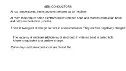
– Hole : It is a seat of positive charge, which is produced when an electron, breaks away from a covalent bond in, a semiconductor. Hole has a positive, charge equal to that of electron., Mobility of hole is smaller than that of, electron., , X, , Insulators, – In insulators, valence band is, completely filled and conduction band, is completely empty., – In insulators, there is a very wide, forbidden energy gap between the, valence and conduction bands. It is of, the order of 5 eV or more., Empty, , X, , Semiconductors, – In semiconductors, valence band is, completely filled and the conduction, band is empty., – In semiconductors, there is a small, forbidden energy gap between the, valence and the conduction bands. It is, of the order of 1 eV. For silicon, it is 1.1, eV and for germanium it is 0.72 eV., , – At absolute zero, semiconductors behave, as a perfect insulator., , Intrinsic semiconductor : A pure semiconductor which is free from every impurity, is known as intrinsic semiconductor., Germanium (Ge) and silicon (Si) are, the important examples of intrinsic, semiconductors., X In intrinsic semiconductor, ne = nh = ni, where ne , nh are number density of, electrons in conduction band and number, density of holes in valence band, ni is the, intrinsic carrier concentration., X When an electric field is applied across, an intrinsic semiconductor, electrons, and holes move in opposite directions so, that total current (I) through the pure, semiconductor is given by, I = Ie + Ih, where Ie is the free electron current and, Ih is the hole current., X Effect of temperature on conductivity, of intrinsic semiconductor, – An intrinsic semiconductor will behave, as a perfect insulator at absolute zero., – With increasing temperature, the, density of hole-electron pairs increases, and hence the conductivity of an, intrinsic semiconductor increases with, increase in temperature. In other words,, the resistivity (inverse of conductivity), decreases as the temperature increases., – The semiconductors have negative, temperature coefficient of resistance., Doping : It is a process of deliberate, addition of a desirable impurity to a pure, semiconductor in order to increase its, conductivity. The impurity atoms added are, known as dopants., Extrinsic semiconductor : A doped, semiconductor is known as extrinsic, semiconductor. Extrinsic semiconductors are, of two types :
Page 3 :
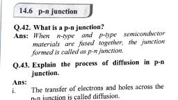
X, , X, , n-type semiconductor, – When a pure semiconductor of Si or, Ge (tetravalent) is doped with a group, V pentavalent impurities like arsenic, (As), antimony (Sb), phosphorus (P), etc, we obtain a n-type semiconductor., The pentavalent impurity atoms are, known as donor atoms., – It is called n-type semiconductor, because the conduction of electricity in, such semiconductor is due to motion of, electrons i.e., negative charges., – It is called donor type semiconductor,, because, the, doped, impurity, atom donates one free electron to, semiconductor for conduction., – In n-type semiconductor electrons, are majority carriers and holes are, minority carriers., – The, representation, of, n-type, semiconductor is as shown in the figure., , – n-type semiconductor is neutral., – In n-type semiconductor, ne ≈ Nd > > nh, where Nd is the density of donor atoms., p-type semiconductor : When a pure, semiconductor of Si or Ge (tetravalent) is, doped with a group III trivalent impurities, like aluminium (Al), boron (B), indium, (In) etc, we obtain a p-type semiconductor., The trivalent impurity atoms are known, as acceptor atoms., – It is called p-type, because the, conduction of electricity in such, semiconductor is due to motion of holes, i.e., positive charges., – It is called acceptor type semiconductor, because the doped impurity atom, creates, a hole in semiconductor, which accepts the electron, resulting, conduction in p-type semiconductor., – In p-type semiconductor, holes are, majority carriers and electrons are, minority carriers., – The, representation, of, p-type, semiconductor is as shown in the figure., , – p-type semiconductor is neutral., – In p-type semiconductor, nh ≈ Na > > ne, where Na is the density of acceptor atoms., Mass action law : Under thermal equilibrium,, the product of the free negative and positive, concentrations is a constant independent of, the amount of donor and acceptor impurity, doping. This relationship is known as the, mass action law and is given by, nenh = ni2, where ne , nh are the number density of, electrons and holes respectively and ni is the, intrinsic carriers concentration., X Electrical conductivity in semiconductor :, The conductivity of the semiconductor is, given by s = e(neme + nhmh), where me and mh are the electron and hole, mobilities, ne and nh are the electron and, hole densities, e is the electronic charge., – The conductivity of an intrinsic, semiconductor is si = nie(me + mh), – The conductivity of n-type, semiconductor is sn = eNdme, – The conductivity of p-type, semiconductor is sp = eNamh, p-n junction : When donor impurities, are introduced into one side and acceptors, into the other side of a single crystal of an, intrinsic semiconductor, a p-n junction is, formed. It is also known as junction diode., The most important characteristic of a p-n, junction is its ability to conduct current in, one direction only. In the other (reverse), direction it offers very high resistance. It is, symbolically represented by, , X, , Depletion region : In the vicinity, of junction, the region containing the, uncompensated acceptor and donor ions, is known as depletion region. There is a, depletion of mobile charges (holes and, free electrons) in this region. Since this, region has immobile (fixed) ions which
Page 4 :
X, , X, , X, , are electrically charged it is also known as, the space charge region. The electric field, between the acceptor and the donor ions is, known as a barrier. The physical distance, from one side of the barrier to the other, is known as the width of the barrier. The, difference of potential from one side of the, barrier to the other side is known as the, height of the barrier., – For a silicon p-n junction, the barrier, potential is about 0.7 V, whereas, for a germanium p-n junction it is, approximately 0.3 V., – The width of the depletion layer and, magnitude of potential barrier depend, upon the nature of the material of, semiconductor and the concentration, of impurity atoms. The thickness of the, depletion region is of the order of one, tenth of a micrometre., Forward biasing of a p-n junction :, When the positive terminal of external, battery is connected to p-side and negative, to n-side of p-n junction, then the p-n, junction is said to be forward biased., – In forward biasing, the width of the, depletion region decreases and barrier, height reduces., – The resistance of the p-n junction, becomes low in forward biasing., Reverse biasing of a p-n junction :, When the positive terminal of the, external battery is connected to n-side, and the negative terminal to p-side of a, p-n junction, then the p-n junction is said, to be reverse biased., – In reverse biasing, the width of the, depletion region increases and barrier, height increases., – The resistance of the p-n junction, becomes high in reverse biasing., Breakdown voltage : A very small, current flows through p-n junction, when, it is reverse biased. The flow of the current, is due to the movement of minority charge, carriers. The reverse current is almost, independent of the applied voltage., However, if the reverse bias voltage is, continuously increased, for a certain, reverse voltage, the current through the, , X, , p-n junction will increase abruptly. This, reverse bias voltage is thus known as, breakdown voltage. There can be two, different causes for the breakdown. One is, known as zener breakdown and the other, is known as avalanche breakdown., I-V characteristics of a p-n junction :, The I-V characteristics of a p-n junction, do not obey Ohm’s law. The I-V, characteristics of a p-n junction are as, shown in the figure., , – Knee voltage : In forward biasing,, the voltage at which the current starts, to increase rapidly is known as cut-in, or knee voltage. For germanium it is, 0.3 V while for silicon it is 0.7 V., – Dynamic resistance : It is defined as, the ratio of a small change in voltage (DV), applied across the p-n junction to a, small change in current DI through the, junction., ∆V, rd =, ∆I, Ideal diode : A diode, permits only unidirectional, conduction. It conducts well, in the forward direction, and poorly in the reverse, direction. It would have been ideal if a diode, acts as a perfect conductor (with zero voltage, across it) when it is forward biased, and as, a perfect insulator (with no current flows, through it) when it is reverse biased. The I-V, characteristics of an ideal diode as shown in, figure., X An ideal diode acts like an automatic, switch.
Page 5 :
X, , In forward bias, it acts as a closed switch, whereas in reverse bias it acts as an open, switch as shown in the figure., , X, , Rectifier : It is a device which converts, ac voltage to dc voltage. Diode is used as a, rectifier. Rectifier is based on the fact that,, a forward bias p-n junction conducts and a, reverse bias p-n junction does not conduct., X Half wave rectifier : Diode conducts, corresponding to positive half cycle and, does not conduct during negative half, cycle. Hence, AC is converted by diode into, undirectional pulsating DC. This action is, known as half-wave rectification., , X, , X, , r=, , 2, , I, , r = rms − 1, Idc , Special Purpose p-n Junction Diodes :, X Light emitting diode (LED) : It converts, electrical energy into light energy. It is a, heavily doped p-n junction which operates, under forward bias and emits spontaneous, radiation., – The I-V characteristics of a LED is, similar to that of Si junction diode. But, the threshold voltages are much higher, and slightly different for each colour., The reverse breakdown voltages of, LEDs are very low, typically around 5 V., – The semiconductor used for fabrication, of visible LEDs must at least have, a band gap of 1.8 eV. The compound, semiconductor, gallium, arsenide, phosphide (GaAsP) is used for making, LEDs of different colours. GaAs is used, for making infrared LED., – The symbol of a LED is shown in the, figure., , X, , Photodiode : A photodiode is a special, type p-n junction diode fabricated with a, transparent window to allow light to fall, on the diode. It is operated under reverse, bias. When it is illuminated with light of, photon energy greater than the energy, gap of the semiconductor, electron-hole, pairs are generated in near depletion, region., – The symbol of a photodiode is shown in, the figure below., , X, , Solar cell : It converts solar energy into, electrical energy. A solar cell is basically, a p-n junction which generates emf when, solar radiation falls on the p-n junction. It, works on the same principle (photovoltaic, effect) as the photodiode, except that no, external bias is applied and the junction, area is kept large., , Full wave rectifier : The circuit diagram,, input and output waveforms for a full, wave rectifier are as shown in the figure., , Ripple factor : The ripple factor is a, measure of purity of the dc output of a, rectifier, and is defined as, , rms value of the components of wave, average or dc value
Page 6 :
1. The equivalent resistance of the circuit, shown in figure between the points A and B if, VA < VB is �, 20 �, (a) 10 W, (b) 20 W, A, B, (c) 5 W, (d) 40 W, 20 �, 2. Which of the following statements is correct?, (a) Hole is an antiparticle of electron., (b) Hole is a vacancy created when an electron, leaves a covalent bond., (c) Hole is the absence of free electrons., (d) Hole is an artificially created particle., 3. Which of the following statements is, incorrect for the depletion region of a diode?, (a) There are mobile charges exist., (b) Equal number of holes and electrons exist,, making the region neutral., (c) Recombination of holes and electrons has, taken place., (d) None of these., 4. In an unbiased p-n junction, holes diffuse, from the p-region to n-region because, (a) free electrons in the n-region attract them, (b) they move across the junction by the, potential difference, (c) hole concentration in p-region is more as, compared to n-region, (d) all of these., 5. A potential barrier of 0.3 V exists across, a p-n junction. If the depletion region is 1 mm, wide, what is the intensity of electric field in, this region?, (a) 2 × 10⁵ V m–1, (b) 3 × 10⁵ V m–1, (c) 4 × 10⁵ V m–1, (d) 5 × 10⁵ V m–1, 6. The dominant mechanism for motion of, charge carriers in forward and reverse biased, silicon p-n junction are, , (a) drift in forward bias, diffusion in reverse, bias, (b) diffusion in forward bias, drift in reverse, bias, (c) diffusion in both forward and reverse bias, (d) drift in both forward and reverse bias., 7. When the voltage drop across a p-n, junction diode is increased from 0.65 V to, 0.70 V, the change in the diode current is, 5 mA. The dynamic resistance of the diode is, (a) 20 W, (b) 50 W (c) 10 W, (d) 80 W, 8. In the circuit shown if drift current for the, diode is 20 mA, the potential, 4V, difference across the diode is, (a) 2 V, 15 �, (b) 4.5 V, (c) 4 V, (d) 2.5 V, 9. If a small amount of antimony is added to, germanium crystal, (a) its resistance is increased, (b) it becomes a p-type semiconductor, (c) there will be more free electrons than holes, in the semiconductor, (d) none of these., 10. A sinusoidal voltage of rms value 220 V is, applied to a diode and a resistor R in the circuit, shown in figure, so that half wave rectification, occurs. If the diode is ideal, what is the rms, voltage across R1?, , (a) 55 2 V, (c) 110 2 V, , (b) 110 V, (d) 220 2 V, , 11. If the energy of a proton of sodium light, (l = 589 nm) equals the band gap of
Page 7 :
semiconductor, the minimum energy required to, create hole electron pair, (a) 1.1 eV, (b) 2.1 eV (c) 3.2 eV (d) 1.5 eV, 12. Which of the following circuits provides full, wave rectification of an ac input?, , (a), , (b), , (c), , (c) Eg(T) = 1.10 – 3.60 × 10⁻⁴T eV, (d) Eg(T) = 1.10 + 3.60 × 10⁻⁴T eV, 16. The maximum wavelength of electromagnetic, radiation, which can create a hole-electron pair, in germanium. (Given that forbidden energy gap, in germanium is 0.72 eV), (a) 1.7 × 10⁻⁶ m, (b) 1.5 × 10⁻⁵ m, –4, (c) 1.3 × 10 m, (d) 1.9 × 10 –5 m, 17. The circuit shown, D1, in the figure contains, D2, two diodes each with a, forward resistance of, 30 W and with infinite, backward resistance. If, the battery is 3 V, the, current through the 50 W resistance (in ampere), is, (a) zero, (b) 0.01, (c) 0.02, (d) 0.03, 18. Which of the junction diodes shown below, are forward biased?, (a), , (b), , (c), , (d), , (d), , 13. Carbon, silicon and germanium have four, valence electrons each. These are characterised, by valence and conduction bands separated by, energy band gap respectively equal to (E g) C,, (E g ) Si and (E g ) Ge . Which of the following, statements is true?, (a) (Eg)Si < (Eg)Ge < (Eg)C, (b) (Eg)C < (Eg)Ge < (Eg)Si, , 19. A potential barrier of 0.50 V exists in a p-n, junction. If the depletion region is 5.0 × 10⁻⁷ m, thick, what is the electric field in this region?, (a) 1 × 10³ V m–1, (b) 1.0 × 10⁶ V m–1, 2, –1, (c) 1 × 10 V m, (d) 1 × 10⁴ V m–1, , (d), , 20. The breakdown in a reverse biased p-n, junction diode is more likely to occur due to, (a) large velocity of the minority charge carriers, if the doping concentration is small, (b) large velocity of the minority charge carriers, if the doping concentration is large, (c) strong electric field in a depletion region if, the doping concentration is small, (d) none of these, , 15. Which of the following equations correctly, represents the temperature variation of energy, gap between the conduction and valence bands, for Si?, (a) Eg(T) = 0.70 – 2.23 × 10⁻⁴T eV, (b) Eg(T) = 0.70 + 2.23 × 10⁻⁴T eV, , 21. In a full wave junction diode rectifier the, input ac has rms value of 20 V. The transformer, used is a step up transformer having primary, and secondary turn ratio 1 : 2. The dc voltage, in the rectified output is, (a) 12 V, (b) 24 V (c) 36 V, (d) 42 V, , (c) (Eg)C > (Eg)Si > (Eg)Ge, (d) (Eg)C = (Eg)Si = (Eg)Ge, 14. A forward biased diode is, (a), (b), (c)
Page 8 :
23. A semiconductor has equal electron and, hole concentration of 6 × 10⁸ per m3. On doping, with certain impurity, electron concentration, increases to 9 × 10 12 per m 3 . The new hole, concentration is, (a) 2 × 10⁴ per m3, (b) 2 × 10² per m2, 4, 3, (c) 4 × 10 per m, (d) 4 × 10² per m3, 24. A p-n photodiode is made of a material with, a band gap of 2 eV. The minimum frequency, of the radiation that can be absorbed by the, material is nearly (Take hc = 1240 eV nm), (a) 1 × 10¹⁴ Hz, (b) 20 × 1014 Hz, 14, (c) 10 × 10 Hz, (d) 5 × 10¹⁴ Hz, 25. A p-n photodiode is fabricated from a, semiconductor with a band gap of 2.5 eV. The, signal wavelength is, (a) 6000 Å, (b) 6000 nm, (c) 4000 nm, (d) 5000 Å, 26. Potential barrier developed in a junction, diode opposes the flow of, (a) minority carrier in both regions only, (b) majority carriers only, (c) electrons in p region, (d) holes in p region, 27. In pure semiconductor, the number of, conduction electrons is 6 × 10¹⁸ per cubic metre., How many holes are there in a sample of size, 1 cm × 1 cm × 1 mm ?, (a) 3 × 10¹⁰, (b) 6 × 10¹¹, 11, (c) 3 × 10, (d) 6 × 10¹⁰, 28. Mobilities of electrons and holes in a sample, of intrinsic germanium at room temperature are, 0.54 m2 V –1 s –1 and 0.18 m2 V –1 s–1 respectively., If the electron and hole densities are equal to, 3.6 × 10 19 m–3, the germanium conductivity is, (a) 4.14 S m–1, (b) 2.12 S m–1, –1, (c) 1.13 S m, (d) 5.6 S m–1, 29. The probability of electrons to be found in the, conduction band of an intrinsic semiconductor of, finite temperature, , (a) increases exponentially with increasing, band gap., (b) decreases exponentially with increasing, band gap., (c) decreases with increasing temperature., (d) is independent of the temperature and band, gap., 30. The electrical conductivity of a semiconductor, increases when electromagnetic radiation of, wavelength shorter than 2480 nm is incident on, it. The band gap (in eV) for semiconductor is, (a) 0.9, (b) 0.7, (c) 0.5, (d) 1.1, 31. The following table provides the set of values, of V and I obtained for a given diode. Let the, characteristics to be nearly linear, over this, range, the forward and reverse bias resistance, of the given diode respectively are, Forward biasing, Reverse biasing, (a) 10 W, 8 × 10⁶ W, (c) 20 W, 8 × 10⁶ W, , V, 2.0 V, 2.4 V, 0V, –2 V, , I, 60 mA, 80 mA, 0 mA, –0.25 mA, , (b) 20 W, 4 × 10⁵ W, (d) 10 W, 10 W, , 32. The mean free path of conduction electrons, in copper is about 4 × 10⁻⁸ m. The electric field, which can give on an average 2 eV energy to a, conduction electron in a block of copper is, (a) 4 × 10⁶ V m–1, (b) 5 × 10⁷ V m–1, 7, –1, (c) 10 × 10 V m, (d) 2.5 × 10⁷ V m–1, 33. The value of ripple factor for full wave, rectifier is, (a) 41%, (b) 141%, (c) 48.2%, (d) 121%, 34. Current through the ideal diode as shown, in figure is, 100 �, , 9, , 22. In a circuit as shown in the, figure, if the diode forward voltage, drop is 0.3 V, the voltage difference, between A and B is, (a) 1.3 V, (b) 2.3 V, (c) 0, (d) 0.5 V, , 2V, , (a) zero, , (b) 20 A, , 5V, , (c), , 1, A, 20, , (d), , 1, A, 50, , 35. In a half wave rectifier circuit operating, from 50 Hz mains frequency, the fundamental, frequency in the ripple would be, (a) 25 Hz, (b) 50 Hz (c) 70.7 Hz (d) 100 Hz
Page 9 :
Case I : Read the passage given below and answer, the following questions from 36 to 40., Biasing of Diode, When the diode is forward biased, it is found, that beyond forward voltage V = Vk, called knee, voltage, the conductivity is very high. At this value, of battery biasing for p-n junction,the potential, barrier is overcome and the current increases, rapidly with increase in forward voltage., When the diode is reverse biased, the reverse, bias voltage produces a very small current about, a few microamperes which almost remains, constant with bias. This small current is reverse, saturation current., 36. In which of the following figures, the p-n, diode is forward biased., , (a), , (b), , (c), , (d), , 37. Based on the V-I characteristics of the diode,, we can classify diode as, (a) bi-directional device, (b) ohmic device, (c) non-ohmic device, (d) passive element, 38. The V-I characteristic of a diode is shown in, the figure. The ratio of forward to reverse bias, resistance is, I (mA), 20, 15, 10, –10, 1 µA, , (a) 100, , (b) 106, , 0.7, , 0.8 V(volt), , (c) 10, , (d) 10–6, , 39. In the case of forward biasing of a p-n, junction diode, which one of the following figures, correctly depicts the direction of conventional, current (indicated by an arrow mark)?, (a), , –+ n, p –, +, –+, , (b), , –+ n, p –, +, –+, , (c), , –+ n, p –, +, –+, , (d), , –+ n, p –, +, –+, , 40. If an ideal junction diode is connected as, shown, then the value of the current I is, I, , (a) 0.013 A, (c) 0.01 A, , (b) 0.02 A, (d) 0.1 A, , Case II : Read the passage given below and, answer the following questions from 41 to 43., Photodiode, A photodiode is an optoelectronic device in, which current carriers are generated by photons, through photo-excitation i.e., photoconduction, by light. It is a p-n junction fabricated from a, photosensitive semiconductor and provided with, a transparent window so as to allow light to fall, on its junction. A photodiode can turn its current, ON and OFF in nanoseconds. So, it can be used, as a fastest photo-detector., Anode, , hu, p n, , Cathode, , 41., (a), (b), (c), , Photodiode is a device, which is always operated in reverse bias., which is always operated in forward bias., in which photocurrent is independent of, intensity of incident radiation., (d) which may be operated in both forward or, reverse bias., 42. To detect light of wavelength 500 nm,, the photodiode must be fabricated from a, semiconductor of minimum bandwidth of, (a) 1.24 eV, (b) 0.62 eV, (c) 2.48 eV, (d) 3.2 eV
Page 10 :
43. Photodiode can be used as a photodetector, to detect, (a) optical signals, (b) electrical signals, (c) both (a) and (b), (d) none of these., Case III : Read the passage given below and, answer the following questions from 44 to 48., p-n Junction Diode, A silicon p-n junction diode is connected to a, resistor R and a battery of voltage VB through a, milliammeter (mA) as shown in figure. The knee, voltage for this junction diode is VN = 0.7 V. The, p-n junction diode requires a minimum current, of 1 mA to attain a value higher than the knee, point on the I-V characteristics of this junction, diode. Assuming that the voltage V across the, junction is independent of the current above the, knee point., A p-n junction is the basic building block of many, semiconductor devices like diodes. Important, process occurring during the formation of a p-n, junction are diffusion and drift. In an n-type, semiconductor concentration of electrons is more, as compared to holes. In a p-type semiconductor, concentration of holes is more as compared to, electrons., , 48. Which of the below mentioned statement is, false regarding a p-n junction diode?, (a) Diodes are uncontrolled devices., (b) Diodes are rectifying devices., (c) Diodes are unidirectional devices., (d) Diodes have three terminals., Case IV : Read the passage given below and, answer the following questions from 49 to 52., Potential Barrier, The potential barrier in the p-n junction diode, is the barrier in which the charge requires, additional force for crossing the region. In other, words, the barrier in which the charge carrier, stopped by the obstructive force is known as the, potential barrier., When a p-type semiconductor is brought into a, close contact with n-type semiconductor, we get, a p-n junction with a barrier potential of 0.4 V, and width of depletion region is 4.0 × 10⁻⁷ m., This p-n junction is forward biased with a, battery of voltage 3 V and negligible internal, resistance, in series with a resistor of resistance, R, ideal millimeter and key K as shown in figure., When key is pressed, a current of 20 mA passes, through the diode., , +, , +, mA, –, , mA, –, , R, , +, VB, , 44., the, (a), (c), , If VB = 5 V, the maximum value of R so that, voltage V is above the knee point voltage is, 40 kW, (b) 4.3 kW, 5.0 kW, (d) 5.7 kW, , 45. If VB = 5 V, the value of R in order to establish, a current to 6 mA in the circuit is, (a) 833 W, (b) 717 W, (c) 950 W, (d) 733 W, , –, 3V, , K, , 49. The intensity of the electric field in the, depletion region when p-n junction is unbiased, is, (a) 0.5 × 10⁶ V m–1, (b) 1.0 × 10⁶ V m–1, 6, –1, (c) 2.0 × 10 V m, (d) 1.5 × 10⁶ V m–1, 50. The resistance of resistor R is, (a) 150 W, (b) 300 W, (c) 130 W, (d) 180 W, , 46. If V B = 6 V, the power dissipated in the, resistor R, when a current of 6 mA flows in the, circuit is, (a) 30.2 mW, (b) 30.8 mW, (c) 31.2 mW, (d) 31.8 mW, , 51. If the voltage of the potential barrier is, V0. A voltage V is applied to the input, at what, moment will the barrier disappear?, (a) V < V0, (b) V = V0, (c) V > V0, (d) V << V0, , 47. When the diode is reverse biased with a, voltage of 6 V and Vbi = 0.63 V. Calculate the, total potential., (a) 9.27 V, (b) 6.63 V, (c) 5.27 V, (d) 0.63 V, , 52. If an electron with speed 4.0 × 10⁵ m s–1, approaches the p-n junction from the n-side, the, speed with which it will enter the p-side is, (a) 1.39 × 10⁵ m s–1, (b) 2.78 × 10⁵ m s–1, (c) 1.39 × 10⁶ m s–1, (d) 2.78 × 10⁶ m s–1
Page 11 :
For question numbers 53-60, two statements are given-one labelled Assertion (A) and the other labelled Reason (R)., Select the correct answer to these questions from the codes (a), (b), (c) and (d) as given below., (a) Both A and R are true and R is the correct explanation of A, (b) Both A and R are true but R is NOT the correct explanation of A, (c) A is true but R is false, (d) A is false and R is also false, 53. Assertion (A) : The conductivity of a semiconductor increases with rise of temperature., Reason (R) : On rising temperature covalent, bonds of semiconductor breaks., 54. Assertion (A) : p-n junction diode can be, used even at ultra high frequencies., Reason (R) : Capacitative reactance of a p-n, junction diode increases as frequency increases., 55. Assertion (A) : The resistance of p-n, junction is low when forward biased and is high, when reverse biased., Reason (R) : In reversed biased, the depletion, layer is reduced., 56. Assertion (A) : The direction of diffusion, current in a junction diode is from n-region to, p-region., Reason (R) : The majority current carriers diffuse, from a region of lower concentration to a region of, higher concentration., , 57. Assertion (A) : The resistivity of a semiconductor increases with temperature., Reason (R) : The atoms of a semiconductor, vibrate with larger amplitude at higher, temperatures thereby increasing its resistivity., 58. Assertion (A) : The half-wave rectifier work, only for positive half cycle of ac., Reason (R) : In half-wave rectifier only one, diode is used., 59. Assertion (A) : The ratio of free electrons to, holes in intrinsic semiconductor is greater than, one., Reason (R) : The electrons are lighter particles, and holes are heavy particles., 60. Assertion (A) : In a semiconductor diode,, the reverse biased current is due to drift of free, electrons and holes., Reason (R) : The drift of electrons and holes is, due to thermal excitations., , SUBJECTIVE TYPE QUESTIONS, , Very Short Answer Type Questions (VSA), 1. What is the difference between an n-type, and a p-type extrinsic semiconductor?, 2. What happens to the width of depletion, layer of a p-n junction when it is (i) forward, biased, (ii) reverse biased ?, 3. Why cannot we use Si and Ge in fabrication, of visible LEDs?, 4., , What is the function of a photodiode ?, , 6. In an n-type semiconductor, where does the, donor energy level lies., 7. Can the potential barrier across a p-n, junction be measured by simply connecting a, voltmeter across the junction?, 8. Draw the output waveform across the, resistor., , 5. Name the junction diode whose I-V, characteristics are drawn below :, , A, +1 V, , I, 0, , V, , –1V, Input waveform at A, , V0
Page 12 :
Why are elemental dopants for Silicon or, , 10. How does an increase in doping concentration, , Germanium usually chosen from group XIII or, , affect the width of depletion layer of a p-n, , group XV?, , junction diode?, , 11. The number densities of electrons and hole, in pure Si at 27°C is 2 × 10¹⁶ m–3. When it is, doped with indium, the hole density increases to, 4 × 10²² m–3, find the electron density in doped, silicon., , 16. (a) Mention the important considerations, required while fabricating a p-n junction diode, to be used as a light emitting diode (LED)., (b) What should be the order of band gap of an, LED if it is required to emit light in the visible, range?, , 9., , 12. A 3 V b a t t e r y m a y b e, connected across the points, A and B as shown. Assuming, ideal diode, find the current, supplied by battery if the, positive terminal of the battery, is connected to the point A., , J1, , 10 W, 30 W, , 17. (a) In the following diagram, which bulb out, of B1 and B2 will glow and why?, , J2, A, , B, , 13. Why photodiodes are required to operate in, reverse bias ? Explain., 14. The circuit shown in the figure has two, oppositely connected ideal diodes connected in, parallel. Find the current flowing through each, diode in the circuit., , (b) If the forward voltage in a semiconductor, diode is changed from 0.5 V to 0.7 V, then the, forward current changes by 1.0 mA. Find the, forward resistance of diode junction., 18. Three photo diodes D1, D2 and D3 are made, of semiconductors having band gaps of 2.5 eV,, 2 eV and 3 eV, respectively. Which ones will be, able to detect light of wavelength 6000 Å?, 19. A p-n photodiode is fabricated from a, semiconductor with band gap of 2.8 eV. Can it, detect a wavelength of 6000 nm?, , 12 V, , 15. Draw V-I characteristics of a p-n junction, diode. Explain, why the current under reverse, bias is almost independent of the applied voltage, up to the critical voltage., , 20. What is the current flowing in R 2 in the, circuit shown in figure? Given : R1 = 500 W and, R2 = 1 kW, R1, , 10 V, , 5V, , R2, , Short Answer Type Questions (SA-II), 21. (a) Distinguish between n-type and p-type, semiconductors on the basis of energy band, diagrams., (b) Compare their conductivities at absolute, zero temperature and at room temperature., 22. Name the important process that occur, during the formation of a p-n junction. Explain, , briefly, with the help of a suitable diagram, how, a p-n junction is formed. Define the term ‘barrier, potential’., 23. If each diode in figure has a forward bias, resistance of 25 Ω and infinite resistance in, reverse bias, what will be the values of the, current I1, I2, I3 and I4?
Page 13 :
A, C, E, I1, G, , I4, , 125 Ω, , I3, , 125 Ω, , I2, , 125 Ω, , based on a certain Ga-As-P semiconducting, material whose energy gap is 1.9 eV. Identify the, colour of the emitted light., (iv) Assuming the ideal diode, draw the output, waveform for the circuit given in figure. Explain, the waveform., , B, D, F, , 25 Ω, , H, , 5V, , 24. Suppose a ‘n’-type wafer is created by doping, Si crystal having 5 × 1028 atoms/m3 with 1 ppm, concentration of As. On the surface 200 ppm, Boron is added to create ‘p’ region in this wafer., Considering ni = 1.5 × 10¹⁶ m–3,, (a) Calculate the densities of the charge carriers, in the n and p regions., (b) Comment which charge carriers would, contribute largely for the reverse saturation, current when diode is reverse biased., 25. With the help of a simple diagram, explain, the working of a silicon solar cell giving all three, basic processes involved., , Forward current I (mA), , 50, 40, 30, 20, 10, 0, , 1, , 2, , 3, , 4, , 5, , 5V, , 27. In half-wave rectification, what is the output, frequency if the input frequency is 50 Hz. What, is the output frequency of a full-wave-rectifier, for the same input frequency?, 28. In the following diagram ‘S’ is a semiconductor., Would you increase or decrease the value of R, to keep the reading of the ammeter A constant, when S is heated? Give reason for your answer., V, – +, , A, , S, , R, , 29. (a) Why are Si and GaAs preferred materials, for fabrication in solar cells?, (b) Draw V-I characteristic of solar cell and, mention its significance., 30. Explain, with the help of a circuit diagram,, the working of a photodiode. Write briefly how, it is used to detect the optical signals., 31. The number of silicon atoms per m 3 is, 5 × 10 28 . This is doped simultaneously with, 5 × 10 22 atoms per m 3 of Arsenic and, 5 × 10 20 per m 3 atoms of Indium. Calculate, the number of electrons and holes. Given that, ni = 1.5 × 10¹⁶ m–3. Is the material n-type or, p-type?, , Yellow, Green, Blue, White, , Infrared, Red, Amber, , 26. Direction : Read the following and answer, the questions given below., Light emitting diode is a photoelectric device which, converts electrical energy into light energy. It is, a heavily doped p-n junction diode which under, forward biased emits spontaneous radiation. The, general shape of the I-V characteristics of an, LED is similar to that of a normal p-n junction, diode, as shown. The barrier potentials are much, higher and slightly different for each colour., , 20 sin ωt, , V, , (i) Draw the I-V characteristic of an LED., (ii) Draw the schematic symbol of light emitting, diode (LED)., (iii) An LED is constructed from a p-n junction, , 32. In the case of n-type Si-semiconductor, the, donor energy level is slightly below the bottom of, conduction band whereas in p-type semiconductor,, the acceptor energy level is slightly above the top, of valence band. Explain, giving examples, what, role do these energy levels play in conduction and, valence bands.
Page 14 :
33. An a.c. signal is fed into two circuits ‘X’ and, ‘Y’ and the corresponding output in the two cases, have the waveforms as shown in figure., (a) �Identify the circuits ‘X’ and ‘Y’. Draw their, labelled circuit diagrams., (b) Briefly explain the working of circuit Y., (c) How does the output waveform from circuit, Y get modified when a capacitor is connected, across the output terminals parallel to the load, resistor?, , 36. (a) In the following diagram, is the junction, diode forward biased or reverse biased?, ., (b) �The V-I characteristic of a silicon diode is, as shown in the figure. Calculate the, resistance of the diode at (i) I = 15 mA and, (ii) V = –10 V, , 34. Draw the circuit arrangement for studying, the V-I characteristics of a p-n junction diode in, (i) forward and (ii) reverse bias. Briefly explain, how the typical V-I characteristics of a diode are, obtained and draw these characteristics., 35. Draw the circuit diagram of a p-n diode used, as a half-wave rectifier. Explain its working., , OBJECTIVE TYPE QUESTIONS, 1. (b) : When VA < VB, the diode gets reverse biased and, offers infinite resistance. No current flows through the upper, branch, \ R = 20 W, 2. (b) : A vacancy created when an electron leaves a, covalent bond. This vacancy is known as hole., 3., , (a) , , 4. (c) : In an unbiased p-n junction, the diffusion of charge, carriers across the junction takes place from higher, concentration to lower concentration. Thus, option (c) is, correct., 5., , (b) : Electric field, V, 0.3, E= =, = 3 × 10⁵ V m–1, d 1 × 10⁻⁶, , (c) : Dynamic resistance, rd =, , −3, , =, , 9. (c) : Adding fifth group element to germanium makes it, an n-type semiconductor. Antimony is a fifth group element, and so germanium becomes n-type semiconductor., 10. (c), hc 6.6 × 10−34 × 3 × 108, 11. (b) : Using, E = Eg =, =, J, λ, 589 × 10−9, =, , 6.6 × 10−34 × 3 × 108, , 589 × 10−9 × 1.6 × 10−19, , eV = 2.1 eV, , 12. (d) 13. (c), , 6. (b) : In p-n junction, the diffusion of majority carriers, takes place when junction is forward biased and drifting of, minority carriers takes place across the junction, when it is, reverse biased., 7., , 0.7 V − 0.65 V, , 0.05 × 1000, Ω = 10 Ω, 5, 5 × 10 A, 8. (c) : Since the diode is reversed biased, only drift current, exists in circuit which is 20 mA. Potential drop across 15 W, resistor, = 15 W × 20 mA = 300 mV = 0.0003 V, Potential difference across the diode = 4 – 0.0003, = 3.99 � 4 V, rd =, , ∆V, ∆I, , 14. (a) : A diode is said to be forward biased if p-type, semiconductor of p-n junction is at high potential with respect, to n-type semiconductor of p-n junction. It is so for circuit (a)., 15. (c) : The energy gap Eg depends on the temperature., For silicon, Eg(T) = 1.10 – 3.60 × 10⁻⁴T eV, For germanium, Eg(T) = 0.70 – 2.23 × 10⁻⁴T eV
Page 15 :
16. (a) : Here, Eg = 0.72 eV = 0.72 × 1.6 × 10–19 J, If l is the maximum wavelength of electromagnetic radiation, which can create a hole-electron pair in germanium, then, hc, Eg =, λ, hc 6.62 × 10−34 × 3 × 108, or λ =, =, = 1.7 × 10⁻⁶ m, Eg, 0.72 × 1.6 × 10−19, 17. (c) : In the circuit, the, upper diode D 1 is reverse, biased and the lower diode D2, is forward biased. Thus there will, be no current across upper diode, junction. The effective circuit will, be as shown in figure., Total resistance of circuit, R = 50 + 70 + 30 = 150 W, 3V, V, = 0.02 A, Current in circuit , I = =, R 150 Ω, 18. (a) : The p-n junction diode is forward biased when p is, at high potential with respect to n. Hence option (a) is correct., V 0.50 V, = 1.0 × 10⁶ V m −1, 19. (b) : Electric field, E = =, d 5 × 10⁻⁷, 20. (b) : In reverse biasing, the minority charge carriers will, be accelerated due to reverse biasing, which on striking with, atoms cause ionisation resulting in secondary electrons and, thus produce more number of charge carriers., When doping concentration is large, there will be large, number of ions in the depletion region, which will give rise, to a strong electric field., 21. (c) : Here, input Vrms = 20 V, Peak value of input voltage, Vo = 2 Vrms = 2 × 20 = 28.28 V, Since the transformer is a step up transformer having, transformer ratio 1 : 2, the maximum value of output voltage, of the transformer applied to the diode will be, V0′ = 2 × Vo = 2 × 28.28 V, 2V0′ 2 × 2 × 28.28, =, = 36 V, π, 22 / 7, 22. (b) : Let V be the potential difference between A and, B, then, V – 0.3 = (5 + 5) × 103 × (0.2 × 10–3) = 2, or V = 2 + 0.3 = 2.3 V, 23. (c) : As, nenh = ni2, \, , dc voltage =, , Here, ni = 6 × 10⁸ per m3 and ne = 9 × 10¹² per m3, ∴ nh =, , 8 2, , ni (6 × 10 ), =, = 4 × 10⁴ per m3, ne, 9 × 10¹², , 24. (d) : Here, Eg = 2 eV, Wavelength of radiation corresponding to this energy is, hc 1240 eV nm, λ=, =, = 620 nm, Eg, 2 eV, c 3 × 10⁸ m s−1, 14, Frequency υ = =, λ 620 × 10−9m = 5 × 10 Hz, 25. (d) : The detection occurs only when the energy of, incident photon greater than or equal to the energy band gap, hc, = 2.5 eV, λ, 1240 eV, hc, nm = 496 nm � 5000 Å, ∴ λ=, =, 2.5 eV 2.5 eV, 26. (b) : Potential barrier developed in a junction diode, opposes the majority carriers only., 27. (b) : Here, ne = 6 × 10¹⁸ m–3, Volume of the sample = 1 cm × 1 cm × 1 mm = 10–7 m3, Number of holes in the sample = Number of electrons in, the sample, = ne × V = 6 ×1018 × 10 –7 = 6 × 10¹¹, 28. (a) : As s = e(neme + nhmh) = eni(me + mh), = 1.6 × 10–19 × 3.6 × 1019(0.54 + 0.18) = 4.147 S m–1, 29. (b), hc 1240 eV nm, =, = 0.5 eV, 2480 nm, λ, 31. (c) : For forward biasing,, DV = 2.4 – 2.0 = 0.4 V; DI = 80 – 60 = 20 mA, 0.4, ∆V, ∴ rfb =, =, = 20 Ω, ∆I 20 × 10−3, 30. (c) : Eg =, , For reverse biasing, DV = – 2 – 0 = –2 V, DI = – 0.25 – 0 = – 0.25 mA, −2, rrb =, = 8 × 10⁶ Ω, −6, −0.25 × 10, 32. (b) : The work done on an electron when it moves, through distance, d = eEd, Work done is equal to the energy transferred to the electron, \ eEd = 2 eV, 2V, 2V, ⇒ E=, =, = 5 × 10⁷ V m−1, d 4 × 10⁻⁸ m, 33. (c) : Ripple factor for full wave rectifier = 0.482., Expressed in %, it is 48.2%., 34. (a) : Here, p-n junction is reverse biased. Therefore, the, current flowing through p-n junction is zero., 35. (b) : Since the output voltage obtained in a half-wave, rectifier circuit has single variation in one cycle of ac voltage,, hence the fundamental frequency in the ripple of output, voltage would be 50 Hz.
Page 16 :
36. (c) : The p-n diode is forward biased when p-side is at, a higher potential than n-side., 37. (c), 38. (d) : Forward bias resistance,, ∆V, 0.8 − 0.7, 0.1, R1 =, =, =, = 10, −, 3, ∆I (20 − 10) × 10, 10 × 10−3, 10, = 107, Reverse bias resistance, R2 =, 1 × 10⁻⁶, Then, the ratio of forward to reverse bias resistance,, R1 10, =, = 10−6, R2 107, 39. (d) : In p-region the direction of conventional current is, same as flow of holes., In n-region the direction of conventional current is opposite, to the flow of electrons., 40 (c) : In the given circuit the junction diode is forward, biased and offers zero resistance., 3 V− 1 V, 2V, =, = 0.01 A, \ The current, I =, 200 Ω 200 Ω, 41. (a) : Photodiode is a device which is always operated in, reverse bias., 42. (c) : Let Eg be the required bandwidth. Then, hc, Eg =, λ, Here, hc = 1240 eV nm, l = 500 nm, 1240 eV nm, ∴ Eg =, = 2.48 eV, 500 nm, 43. (a) : A photodiode is a device which is used to detect, optical signals., 44. (b) : Voltage drop across R,, VR = VB – VN = 5 – 0.7 = 4.3 V, Here, Imin = 1 × 10⁻³ A, V, 4.3, \ Rmax = R =, = 4.3 × 10³ Ω = 4.3 kW, Imin 1 × 10⁻³, 45. (b) : I = 6 mA = 6 × 10⁻³ A;, VR = VB – VN = 5 – 0.7 = 4.3 V, V, 4.3, R= R =, = 717 Ω, I 6 × 10⁻³, 46. (d) : Here, VB = 6 V; VN = 0.7 V,, VR = 6 – 0.7 = 5.3 V, Power dissipated in R = I × VR, , = (6 × 10–3) × 5.3 = 31.8 × 10⁻³ W = 31.8 mW, 47. (b) : Vt = Vbi + VR = 0.63 + 6 = 6.63 V, 48. (d) : Diode is two terminal device, anode and cathode, are the two terminals., , 49. (b) : E =, , VB, 0.4, =, = 1.0 × 10⁶ V m−1, d 4.0 × 10⁻⁷, , 50. (c) : Potential difference across R = 3 – 0.4 = 2.6 V, 2.6, Potential difference, =, = 130 Ω, Resistance R =, Current, 20 × 10−3, 51. (b) : When the voltage will be the same as that of the, potential barrier, the potential barrier will disappear resulting, in flow of current., 1, 1, 52. (a) : mv12 = eVB + mv22, 2, 2, 1, −31, ⇒, × (9.1 × 10 ) × (4 × 10⁵ )2, 2, 1, = 1.6 × 10−19 × (0.4) + × 9.1 × 10⁻³¹ × v22, 2, On solving, we get, v2 = 1.39 × 10⁵ m s–1, 53. (c) : At 0 K, all semiconductors are insulators. The, valence band at 0 K is completely filled and there are no, free electrons in conduction band. At room temperature due, to thermal energy, the electron jump to the conduction band., When the temperature increases, a large number of electrons, cross over the forbidden gap and jump from valence band to, conduction band. Thus with rise in temperature conductivity, increases. The covalent bonds of semiconductor breaks, only when it is heated up extremely either by increasing, temperature or by supplying strong current. After which it, behaves like conductor and no longer possesses the property, of low conduction, hence it is said to be damaged., 54. (c) : As capacitative reactance,, 1, 1, 1, XC =, =, i.e., XC ∝, ωC 2πυC, υ, Thus, capacitative reactance decreases on increase in, frequency., 55. (c) : A small increase in forward voltage across p-n, junction shows large increase in forward current. Hence the, resistance (= voltage / current) of p-n junction is low when, forward biased. Also the width of depletion layer of p-n, junction decreases in forward bias., A large increase in reverse voltage across p-n shows small, increase in reverse current. Hence the resistance of p-n, junction is high when reverse biased. Also the width of the, depletion layer of p-n junction increases in reverse biased., 56. (d) : The direction of diffusion current is that when, positively charged particles move from p-type to n-type of, diode., 57. (d) : With the increase of temperature, the average, energy exchanged in a collision increases and so more valence, electrons can cross the energy gap, thereby increasing the, electron-hole pairs. As in a semiconductor, conduction occurs
Page 17 :
mainly through electron-hole pairs, so conductivity increases, with increase of temperature. Which in turn implies that, the resistivity of a semiconductor decreases with rise in, temperature., , 8., , 58. (a) : In half wave rectifier, the one diode is biased only, when ac is in positive half of its cycle. For negative half of the, ac cycle the diode is reversed biased and there is no output, corresponding to that. Since for only one-half cycle we get, a voltage output, because of which it is called half wave, rectifier., , The diode acts as half wave rectifier, it offers low resistance, when forward biased and high resistance when reverse, biased., , 59. (b) : In intrinsic semiconductor n e/n h = 1 and holes, are not particles but vacancies created due to breakage of, covalent bond., 60. (b) : A reverse bias on a p-n junction opposes the, movement of the majority charge carriers thus stopping the, diffusion current. It makes the free electrons and holes to, drift cross the junction. Therefore a small current in mA flows, even when the p-n junction is reverse biased. The drift current, is due to the thermal excitations of the electrons and holes., , SUBJECTIVE TYPE QUESTIONS, 1., , n-type, Semiconductor, , p-type, Semiconductor, , (i), , It is formed by doping, pentavalent impurities., , It is formed by doping, trivalent impurities., , (ii), , The electrons are majority, carriers and holes are, minority carriers., (ne >> nh), , The holes are majority, carriers and electrons, are minority carriers., (nh >> ne), , 2. (i) Forward biased : As forward voltage opposes the, potential barrier and effective barrier potential decreases. It, makes the width of the depletion layer smaller., (ii) Reverse biased : As reverse voltage supports the potential, barrier and effective barrier potential increases. It makes the, width of the depletion layer larger., , +1V, , 0, , 9. Size of the dopant atom should be compatible in the pure, semiconductor and contribute a charge carrier by forming, covalent bond with Si or Ge atoms. Elemental dopants from, group XIII and group XV fulfil this condition., 10. When there is an increase in doping concentration, the, applied potential difference causes an electric field which, acts opposite to the potential barrier. This results in reducing, the potential barrier and hence the width of depletion layer, decreases., 11. For extrinsic or doped semiconductor, ne ⋅ nh = ni2 ⇒ ne =, , Here ni = 2 × 10¹⁶ m–3 and nh = 4 × 10²² m–3, ( 2 × 10¹⁶ m−3 ) 2, , = 10 −10 m−3 ., 4 × 10 22 m−3, 12. If A is positive and B is, negative, J1 is forward biased and, J2 is reverse biased, so effective, current is, ⇒ ia = = 0.3 A., ⇒, , ne =, , 2Ω, , 4. Photodiode is used to detect the light signal and to, measure light intensity., , 4Ω, , 6. (b) : In n-type semiconductor, the donor energy level lies, just below the conduction band., 7. No, the voltmeter should have a very high resistance as, compared to the resistance of p-n junction, which is nearly, infinite., , A, , B, , 14. Diode D 1 is reverse biased,so it offers an infinite, resistance. So no current flows in the branch of diode D1., , D1, , The junction diode is solar cell., , J1, , 13. In reverse bias condition of photodiode, the change, in saturation reverse current is directly proportional to the, change in the incident light flux or light intensity, which can, be measured accurately. It is not so when photodiode is, forward biased., , 3. LED’s must have band gap in the order of 1.8 eV to, 3 eV but Si and Ge have band gap less than 1.8 eV., , 5., , ni2, nh, , D2, , 3Ω, , +, , 12 V, , Diode D2 is forward biased, and offers negligible resistance, in the circuit. So current in the branch, V, 12 V, I=, =, = 2A, R eq 2 Ω + 4 Ω
Page 18 :
15., , 20. The diode is reverse biased, but the voltage across it is, given as 5 V. R2 is in parallel with the diode, so current in R2, 5V, =, ⇒ Current in R2 = 5 mA., 1000 Ω, , z, , 21. (a) The required energy band diagrams are given below:, , The reverse current is due to minority charge carriers and, even a small voltage is sufficient to sweep the minority, carriers from one side of the junction to the other side of the, junction. Here the current is not limited by the magnitude of, the applied voltage but is limited due to the concentration of, the minority carrier on either side of the junction., 16. (a) (i) There is very little resistance to limit the current, in LED. Therefore, a resistor must be used in series with the, LED to avoid any damage to it., (ii) The reverse breakdown voltages of LEDs are very low,, typically around 5 V. So care should be taken while fabricating, a p-n-junction diode so that the p side should only attached, to the positive of battery and vice versa as LED easily get, damaged by a small reverse voltage., (b) The semiconductor used for fabrication of visible LEDs, must have at least a band gap of 1.8 eV because spectral, range of visible light is about 0.4 mm to 0.7 mm, i.e., about, 3 eV to 1.8 eV., 17. (a) Bulb B1 will glow, as diode D1 is forward biased., Bulb B2 will not glow as diode D2 is reverse biased., ∆V, , (b) Forward resistance = ∆I, 0.7 − 0.5, ∆V, ∴, =, −3 = 200 Ω., ∆I, , T>0K, , T>0K, , (b), , at T = 0 K, , At absolute zero temperature (0 K), conduction band of, semiconductor is completely empty, i.e., s = 0. Hence the, semiconductor behaves as an insulator. At room temperature,, some valence electrons acquire enough thermal energy, and jump to the conduction band where they are free to, conduct electricity. Thus the semiconductor acquires a small, conductivity at room temperature., 22. Two processes that take place in the formation of a p-n, junction are diffusion and drift., , 1.0 × 10, , hc, 18. We know that, energy of incident photon, E =, λ, l = 6000 Å = 600 nm (given), 1242 eV nm, = 2.07 eV, 600 nm, D2 will detect these radiations because energy of incident, radiation is greater than the band gap., E =, , 19. Energy of the incident photon with a band gap of, 6000 nm., E=, , 6.63 × 10 −34 × 3 × 10 8, hc, hc, J = eV =, = 0.207 eV, λ, eλ, 1.6 × 10 −19 × 6 × 10 −6, , The photodiode need an energy of 2.8 eV to give response, to incident light., As E < Eg, the given photodiode cannot detect the radiation, of wavelength 6000 nm., , When p-n junction is formed, then at the junction, free, electrons from n-type diffuse over to p-type, thereby filling, in the holes in p-type. Due to this a layer of positive charge is, built on n-side and a layer of negative charge is built on p-side, of the p-n junction. This layer sufficiently grows up within a, very short time of the junction being formed, preventing any, further movement of charge carriers (i.e., electrons and holes), across the junction. Thus a potential difference V0 of the, order of 0.1 to 0.3 V is set up across the p-n junction called, potential barrier or junction barrier. The thin region around the
Page 19 :
junction containing immobile positive and negative charges, is known as depletion layer., 23. Let R be the effective resistance of the circuit, then, R = RAB || REF + 25, RAB = 125 + 25 = 150 W, REF = 125 + 25 = 150 W, 150, \ R = 25 +, = 100 W, 2, Since diode in the branch CD is reverse biased. I3 = 0., 5, Current, I1 =, = 0.05 A, 100, According to Kirchhoff’s current rule,, I1 = I2 + I3 + I4 or I2 + I4 = I1 = 0.05, RAB = REF, so, I4 = I2, 2I4 = 2I2 = 0.05, 0.05, I4 = I2 =, = 0.025 A, 2, 24. (a) For n-type region,, 1, ne = ND = 6 × 5 × 10 28 = 5 × 10²² m–3, 10, 1 , , ∵ 1 ppm = 6 , 10, As nenh = ni2,, ni2 (1.5 × 10¹⁶ m−3 )2, = 0.45 × 10¹⁰ m–3, =, ne, 5 × 10 22 m−3, For p-type region,, 200, nh = NA = 6 × 5 × 10 28 = 1 × 1025 m–3, 10, n 2 (1.5 × 10¹⁶ m−3 )2, Now, ne = i =, = 2.25 × 10⁷ m–3, 25 −3, nh, 1 × 10 m, (b) The minority carrier holes of n-region wafer, (nh = 0.45 × 10¹⁰ m–3) would contribute more to reverse, saturation current than minority carrier electrons of p–region, wafer (ne = 2.25 × 10⁷ m–3) when p – n junction is reverse, biased., nh =, , 25. Principle : A solar cell works on the principle of photovoltaic effect according to which when light photons of, energy greater than energy band gap of a semiconductor are, incident on p-n junction of that semiconductor, electron-hole, pairs are generated which give rise to an emf., Generation of emf : Three basic processes are involved in the, generation of emf by a solar cell when solar radiations are, incident on it. These are:, (i) The generation of electron-hole pairs close to the, junction due to incidence of light with photo energy hu ≥ Eb., (ii) The separation of electrons and holes due to the electric, field of the depletion region. So, electrons are swept to n-side, , and holes to p-side., (iii) The electrons reaching the, n-side are collected by the front, contact and holes reaching p-side, are collected by the back contact., Thus, p-side becomes positive and, n-side become negative giving rise, to a photovoltage., , RL, , When an external load RL is connected as shown in figure, a, photocurrent IL begins to flow through the load., 26. (i) The I-V characteristics of an, LED is similar to that of a Si junction, diode. But the threshold voltages are, much higher and slightly different for, each colour., (ii), , hc, hc, \ λ=, λ, Eg, Here, Eg = 1.9 eV, hc = 1240 eV nm, 1240 eV nm, \ λ=, = 652.6 nm, 1.9 eV, Hence, the emitted light is of red colour., (iv) For the voltage less than 5 V, the diode is reverse biased, and circuit will act as open circuit., When input voltage is greater than 5 V, diode is in conducting, state., (iii) As Eg =, , 27. In half wave rectification, only one ripple is obtained per, cycle in the output.
Page 20 :
Output frequency of a half wave rectifier = input frequency, = 50 Hz, In full wave rectification, two ripples are obtained per cycle, in the output., Output frequency = 2 × input frequency, = 2 × 50 = 100 Hz, , 28. We will increase the value of R. On heating a, semiconductor, its resistance decreases with rise in, temperature. As the semiconductor, S is in series, so net, resistance of the circuit also decreases. So by increasing the, value of R we can keep the resistance of circuit constant and, hence the current in the circuit or the reading of ammeter A, can be kept constant., 29. (a) The energy for the maximum intensity of the solar, radiation is nearly 1.5 eV. In order to have photo excitation, the energy of radiation (hu) must be greater than energy, band gap (Eg), i.e., hu > Eg. Therefore, the semiconductor, with energy band gap about 1.5 eV or lower and with higher, absorption coefficient, is likely to give better solar conversion, efficiency., The energy band gap for Si is about 1.1 eV, while for GaAs, it, is about 1.53 eV. The gas GaAs is better inspite of its higher, bandgap than Si because it absorbs relatively more energy, from the incident solar radiations being of relatively higher, absorption coefficient., (b), (open circuit, voltage), , (i) V-I curve is drawn in the fourth quadrant, because a solar, cell does not draws current but supply current to the load., (ii) In V-I curve, the point A indicates the maximum voltage, VOC being supplied by the given solar cell when no current is, being drawn from it. VOC is called the open circuit voltage., , (iii) In V-I curve, the point B indicates the maximum current, ISC which can be obtained by short circuiting the solar cell, without any load resistance. ISC is called the short circuit, current., 30. Working of photodiode :, h�, A junction diode made from, light sensitive semiconductor is, c a l l e d a p h o t o d i o d e. A, �A, photodiode is a p-n junction, p-side n-side, diode arranged in reverse, R, biasing., The number of charge carriers increases when light of suitable, frequency is made to fall on the p-n junction, because new, electron-hole pairs are created by absorbing the photons of, suitable frequency. Intensity of light controls the number of, charge carriers. Due to this property photodiodes are used, to detect optical signals., 31. We know that for each atom doped with Arsenic, one, free electron is received. Similarly, for each atom doped with, indium, a vacancy is created., So, the number of free electrons introduced by pentavalent, impurity added,, ne = NAs = 5 × 10²² m–3, The number of holes introduced by trivalent impurity added, nh = NIn = 5 × 10²⁰ m–3, We know the relation, nenh = ni2�...(i), Now net electrons,, n′e = ne – nh = 5 × 10²² – 5 × 10²⁰, = 4.95 × 10²² m–3�...(ii), Now using equation (i), net holes, ni 2 (1.5 × 10¹⁶ )2, = 4.5 × 10 9 m−3, =, n ′e, 4.95 × 10 22, So, n′e >> n′h, the material is of n-type., 32. In n-type extrinsic semiconductors, the number of free, electrons in conduction band is much more than the number, of holes in valence band. The donor energy level lies just, below the conduction band. In p-type extrinsic semiconductor,, the number of holes in valence band is much more than the, number of free electrons in conduction band. The acceptor, energy level lies just above the valence band., 33. (a) X = Half wave rectifier, Y = Full wave rectifier, n′h =, , (Half wave rectifier)
Page 21 :
through RL remains same, but its magnitude changes with, time, so it is called pulsating d.c., , (b) Two p–n junction diodes can be used to make full wave, rectifier which is used to convert alternating current into, direct current., Centre- Tap, Transformer, , Diode D1, A, Centre Tap, B, , X, RL Output, , Diode D2, Y, , A full wave rectifier consists of two diodes connected in, parallel across the ends of secondary winding of a center, tapped step down transformer. The load resistance RL is, connected across secondary winding and the diodes between, A and B as shown in the circuit., During positive half cycle of input a.c., end A of the secondary, winding becomes positive and end B negative. Thus diode D1, becomes forward biased, whereas diode D2 reverse biased. So, diode D1 allows the current to flow through it, while diode, D2 does not, and current in the circuit flows from D1 and, through load RL from X to Y., During negative half cycle of input a.c., end A of the secondary, winding becomes negative and end B positive, thus diode D1, becomes reverse biased, whereas diode D2 forward biased., So diode D1 does not allow the current to flow through it, but diode D2 does, and current in the circuit flows from D2, and through load RL from X to Y., , 34. Forward biased characteristics : The circuit diagram for, studying forward biased characteristics is shown in the figure., Starting from a low value, forward bias voltage is increased, step by step (measured by voltmeter) and forward current is, noted (by ammeter). A graph is plotted between voltage and, current. The curve so obtained is the forward characteristic of, the diode., , Current, , (Full wave rectifier), , (c) A capacitor of large capacitance is connected in parallel, to the load resistor RL. When the pulsating voltage supplied, by the rectifier is rising, the capacitor C gets charged. If, there is no external load, the capacitor would have remained, charged to the peak voltage of the rectified output. However,, when there is no load and the rectified voltage starts falling,, the capacitor gets discharged through the load and the, voltage across capacitor begins to fall slowly., , Voltage (V), , Input-Output waveforms, , At the start when applied voltage is low, the current through, the diode is almost zero. It is because of the potential barrier,, which opposes the applied voltage. Till the applied voltage, exceeds the potential barrier, the current increases very slowly, with increase in applied voltage (OA portion of the graph)., With further increase in applied voltage, the current increases, very rapidly (AB portion of the graph), in this situation, the, diode behaves like a conductor. The forward voltage beyond, which the current through the junction starts increasing, rapidly with voltage is called threshold or cut-in voltage. If, line AB is extended back, it cuts the voltage axis at potential, barrier voltage., , Since in both the half cycles of input a.c., electric current, through load R L flows in the same direction, so d.c. is, obtained across RL. Although direction of electric current, , Reverse biased characteristics : The circuit diagram, for studying reverse biased characteristics is shown in the, figure., , Vin, O, , t, , Vout, t, , O
Page 22 :
Primary of transformer is connected to a.c. supply. During, positive half cycle of input a.c., end A of the secondary, winding becomes positive and end B negative. Thus, diode, D becomes forward biased and conducts the current through, it. So, current in the circuit flows from A to B through load, resistor RL., , Current �, , Voltage (V), , In reverse biased, the applied voltage supports the flow of, minority charge carriers across the junction. So, a very small, current flows across the junction due to minority charge, carriers., Motion of minority charge carriers is also supported by, internal potential barrier, so all the minority carriers cross, over the junction., Therefore, the small reverse current remains almost constant, over a sufficiently long range of reverse bias, increasing very, little with increasing voltage (OC portion of the graph). This, reverse current is voltage independent upto certain voltage, known as breakdown voltage and this voltage independent, current is called reverse saturation current., 35. Half wave rectifier:, , During negative half cycle of input a.c., end A of the secondary, winding becomes negative and end B positive. Thus, diode D, becomes reverse biased and does not conduct any current. So,, no current flows in the circuit. Since electric current through, load RL flows only during positive half cycle, in one direction, only i.e., from A to B, so d.c. is obtained across RL., 36. (a) Voltage at p side is less than voltage at n side of, the diode so it is in reverse bias., (b) (i) From the given curve, we have, voltage, V = 0.8 volt for current, I = 20 mA, voltage, V = 0.7 volt for current, I = 10 mA, ⇒ DI = (20 – 10)mA = 10 × 10–3 A, ⇒ DV = (0.8 – 0.7) = 0.1 V, 0.1, ∆V, \ Resistance, R =, ⇒ R=, ⇒ R = 10 W, ∆I, 10 × 10 −3, (ii) For V = – 10 V, we have, , It consists of a diode D connected in series with load resistor, RL across the secondary windings of a step-down transformer., , I = – 1 mA = –1 × 10⁻⁶ A ⇒ R =, , , , 10, 1 × 10 −6, , = 1.0 × 10 7 Ω
 Learn better on this topic