Notes of CLASS : 11th, PHYSICS Semiconductor Electronics.pdf - Study Material
Page 1 :
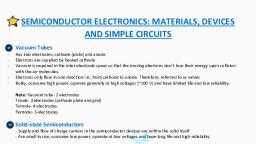
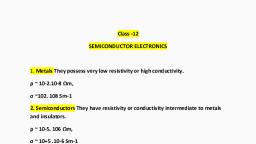
Chapter 14, , Semiconductor Electronics :, Materials, Devices and Simple Circuits, , Chapter Contents, , Introduction, , Classification of Metals,, Conductors and, Semiconductors, , Classification of Solids on, the Basis of Energy Bands, , Intrinsic Semiconductor, p-n Junction, Semiconductor Diode, , Application of Junction, Diode as a Rectifier, , Special Purpose p-n, Junction Diodes, , Junction Transistor, Digital Electronics and Logic, Gates, , Integrated Circuits, Some Important Definitions, Formulae Chart, , Quick Recap, , Introduction, , Controlled flow of electrons are the basic bullding blocks of all the, electronic circuits. Vacuum tube diode valves were fabricated as the, first-generation electronic circuit component which dominated till, 1950. After 1950 all vacuum tube-based electronic circuits were, replaced by semiconductor transistors and they were called secondgeneration circults. Then came ‘Integrated Circuits’ (ICs) which made, the circuits further smaller., , In this chapter first we will discuss band theory of solids. Then we will, discuss junction diode and transistors. After that we will explore the, basics of Logic gates. At the end we will take the elementary idea of, integrated circuits., , CLASSIFICATION OF METALS, CONDUCTORS AND, SEMICONDUCTORS, , Classification of solids on the basis of conductivity, , On the basis of this criterion, solids are classified as metals, semiconductors, and insulators. Metals possess very low resistivity (10-2 to 10° Om) or high, conductivity (10? to 108 Sm"), Semiconductors have resistivity (10-5 to 10®, Qm) or conductivity (10° to 10° Sm") intermediate to metals and insulators., Insulators have high resistivity (10"' to 10’? Qm) or low conductivity (10-1!, to 10-'® Sm). Note that the values of resistivity or conductivity are, approximate., , In this chapter we will concentrate mainly on semiconductors which could, be “Elemental Semiconductors” (e.g., Si and Ge) and “Compound, Semiconductors”. Compound Semiconductors can be “inorganic” (e.g., CdS,, GaAs, CdSe, InP etc.); ‘organic’ (e.g., anthracene, doped pthalocyanines,, etc.) and ‘Organic Polymer’ (@.g., polypyrrole, polyaniline, polythiophene etc.)., We will restrict ourselves to the study of inorganic semiconductors,, particularly elemental semiconductors, Si and Ge., , , , Aakash Educational Services Pvt. Ltd. - Regd. Office : Aakash Tower, 8, Pusa Road, New Deihi-110005 Ph. 011-47623456
Page 2 :
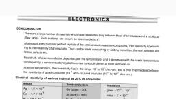
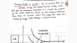
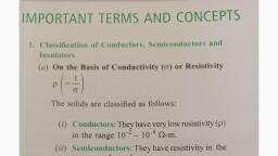
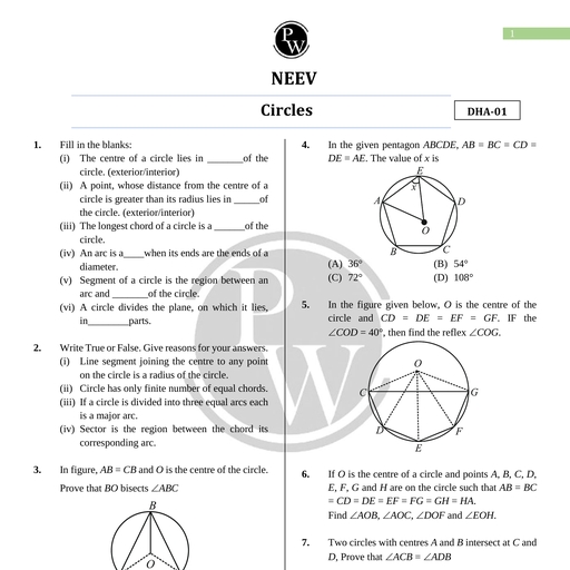
338 Semiconductor Electronics : Materials, Devices and Simple Circuits Board & Competitive Exams., , , , CLASSIFICATION OF SOLIDS ON THE BASIS OF ENERGY BANDS, , Bohr's atomic model suggests that in an isolated atom the energy of its electron is decided by the orbit in, which it revolves. But in a solid the situation is very different. When the atoms come together to form a solid, they are so close to each other that the fields of electrons of outer orbits from neighbouring atoms overlap., This makes the nature of electron motion in a solid very different from that in an isolated atom. Inside the, solid (crystal), each electron has a unique position and no two electrons have same pattern of surrounding, charges. Hence, each electron has a different energy level. These energy levels are so closely packed that, we call it energy band. The energy band which includes the energy levels of the valence electrons is called, the valence band. The higher energy band (above the valence band) is called the conduction band. With no, extemal energy, all the valence electrons stay in the valence band. In metallic conductors the lowest level, of the conduction band happens to be lower than the highest level of the valence band. Hence, the electrons, from the valence band can easily move into the conduction band. Normally the conduction band is empty but, when it overlaps on the valence band, electrons can move freely into it., , In insulators, there is some energy gap between the conduction band and the valence band. Electrons in the, valence band remain bonded and no free electrons are available in the conduction band. Hence, it behaves, like an insulator. But if some external energy is provided then some of the electrons from the valence band, may jump across the energy gap between the conduction band and the valence band to move into the, conduction band. This jumping of electrons creates vacant energy levels in the valence band where other, valence electrons can enter. Hence, this jumping process creates the mechanism of conduction due to, electrons in the conduction band as well as conduction of electrons into the vacancies in the valence band., , In the figure below, the lowest energy level in the conduction band is shown as E,, and highest energy level, in the valence band is shown as E,. Above E, and below £,, there are a large number of closed spaced, energy levels., , , , , , , , , , =, , Infinitely large number of, , States each occupied by, , two electrons, Fig. : The energy band positions in a semiconductor at 0 K. The upper band, called the conduction band,, consists of infinitely large number of closely spaced energy states. The lower band, called the valence band,, consists of closely spaced completely filled energy states., , The gap between the top of the valence band and bottom of the conduction band is called the energy band, gap (energy gap £,). It may be large, small or zero depending upon the material discussed below., , Case | : (For metals), , In metals two types of situations are possible. In first case, we can have a metal whose conduction band is, partially filled and the valence band is partially empty. In second case, we can have conduction band and, valence band overlapping each other. When there is the case of overlapping then electrons from valence band, can easily move into the conduction band which makes a large number of electrons available for electrical, conduction. When the valence band is partially empty then electrons from lower energy levels in it try to fill, this gap resulting into the movement of electrons and hence, conduction takes place. This explains why the, resistance of such materials is low or the conductivity is high., , Aakash Educational Services Pvt. Ltd. - Regd. Office : Aakash Tower, 8, Pusa Road, New Deihi-110005 Ph. 011-47623456
Page 3 :
Board & Competitive Exams. Semiconductor Electronics : Materials, Devices and Simple Circuits 339, , J nico band, , ms, , E, band (E, = 0), SIE, , ‘| ss al* =, , band, @ (il), , Difference between energy bands of metals, , Case Il : (For insulators), , In case of insulators, a large energy band gap E, exists between the valence band and conduction band., (E > 3 eV). There are no electrons in the conduction band and hence, electrical conduction is not possible, under ordinary circumstances. It means that the energy gap is so large that electrons cannot be excited from, the valence band to the conduction band by thermal excitation., , , , , , Empty —, E: conduction, 8 6 band, = E,>3ev, i * Valence, band, , Difference between energy bands of insulators, Case Ill : (For Semiconductors), In semiconductors, a small and finite energy band gap (E, <3 eV) exists. Because of the small energy band, gap some electrons from valence band, at room temperature, acquire enough energy to cross the energy gap, , and enter the conduction band. These electrons are very few and can move in the conduction band. Hence,, the resistance of semiconductors is not as high as that of the insulators., , , , £ E, : E,<3ev, i P, Difference between energy, bands of semiconductors, os, Example 1: The energy gap of silicon is 1.14 eV. What is the maximum wavelength at which silicon will begin, absorbing energy?, he, Solution : SE, , _ 6.628x10™ (J-s)x 3x 10°(m/s), 1.14x1.6x107-" J, 10.901 x 10⁻⁷ m, , 10901 A, , , , Aakash Educational Services Pvt. Ltd. - Regd. Office : Aakash Tower, 8, Pusa Road, New Deihi-110005 Ph. 011-47623456
Page 4 :
340 Semiconductor Electronics : Materials, Devices and Simple Circuits Board & Competitive Exams., , Try Yourself, , 1. In semiconductors at room temperature the, (1) Valence band is partially empty and the conduction band is partially filled, (2) Valence band is completely filled and the conduction band is partially empty, (3) Valence band is completely filled, (4) Conduction band is completely empty, , 2. Carbon, silicon and germanium atoms have four valence electrons each. Their valence and, , conduction bands are separated by energy band gaps represented by (E,)c, (E,)s, and (E,)ae, Sa aa, , 1) Ege > (Es: 2) (Ege = (Eqs:, @) (Ede < (Eee (4) = eee, , , , , , , , Energy Band Description of Solids, , In a single free atom, electrons have well-defined energy levels. In a crystal, there are many atoms. So, an, atom in a crystal is surrounded by neighbouring atoms, and due to the interaction of these atoms, the energy, levels of electrons of the atom are modified. The energy levels of the innermost shell are not modified but, the energy levels of the outer shells are modified too much because these electrons are loosely bound to, the nucleus and the electron interaction of different atoms is too much for the outer electrons., , Consider a single small crystal of silicon made of N atoms. The electronic configuration of silicon crystal is, 1s? 2s? 2p® 3s? 3p?. The outer shell contains 2 electrons in 3s sub-shell and 2 electrons in 3p subshell. The, 2N s-evels (all at the same energy) in the outermost shell are completely filled by 2N electrons but out of, 6N available 3p sub-shells only 2N sub-shells are filled and 4N are empty., , Figure shows the energy levels in silicon atoms. The actual interatomic separation in silicon atoms is denoted, by r= a. In order to understand the process of modification of energy levels, let us imagine that silicon atoms, are brought near each other from very far away distance and they finally occupy their actual locations, (r = a) in the crystal lattice. nagond, , Aa, 4N States Ni (lootsted stome), , , , , , , , , , , , , , ae (.-1", =o shell, , Aakash Educational Services Pvt. Ltd. - Regd. Office : Aakash Tower, 8, Pusa Road, New Dethi-110005 Ph. 011-47623456
Page 5 :
Board & Competitive Exams. Semiconductor Electronics : Materials, Devices and Simple Circuits 341, , INTRINSIC SEMICONDUCTOR, , Structure : Most common case of semiconductors is that of Ge and Si whose lattice structures are called the, diamond-like structures. In this structure each atom is surrounded by four nearest neighbours. Si and Ge have, four valence electrons. In its crystalline structure, every Si or Ge atom tends to share one of its four valence, electrons with each of its four nearest neighbour atoms. These shared electrons form covalent bond (also called, valence bond). The two shared electrons move back and forward between the associated atoms holding them, together strongly. Figure shows the schematic two-dimensional representation of Si and Ge structure., , , , Fig. : Schematic two-dimensional representation of Si or Ge structure showing, covalent bonds at low temperature (all bonds intact). +4 symbol indicates inner cores of Si or Ge., , This is an ideal picture in which no bonds are broken and all bonds are intact. Such a situation exists at, low temperature., Conduction process in semiconductors, , As the temperature of these semiconductor increases some of these bonded electrons gain thermal energy, and become free. These free electrons and vacancy in bond contribute to conduction of electricity in, semiconductors. The thermal energy is able to ionize only a few atoms in the crystalline lattice and creates, a vacancy in the bond as shown in figure (a)., , @ (Thermalty generated free electron), , , , Fig. : (a) Schematic model of generation of hole at site 1 and conduction electron due to thermal, energy at moderate temperatures. (b) Simplified representation of possible thermal motion of a hole., , The electron from the lower left hand covalent bond (site 2) goes to the earlier hole site 1,, , leaving a hole at its site indicating an apparent movement of the hole from site 1 to site 2., , The surroundings from which the free electron with charge (—q) has come out leaves a gap or vacancy with, an effective charge (+q). This vacancy, with the effective positive electronic charge is called a ‘hole’. The hole, appears to behave as free particle with effective positive charge., , Aakash Educational Services Pvt. Ltd. - Regd. Office : Aakash Tower, 8, Pusa Road, New Delhi-110005 Ph. 011-47623456
 Learn better on this topic