Notes of Xll ScienceABC NSB, Physics & Physics semiconductor diode.pdf - Study Material
Page 2 :
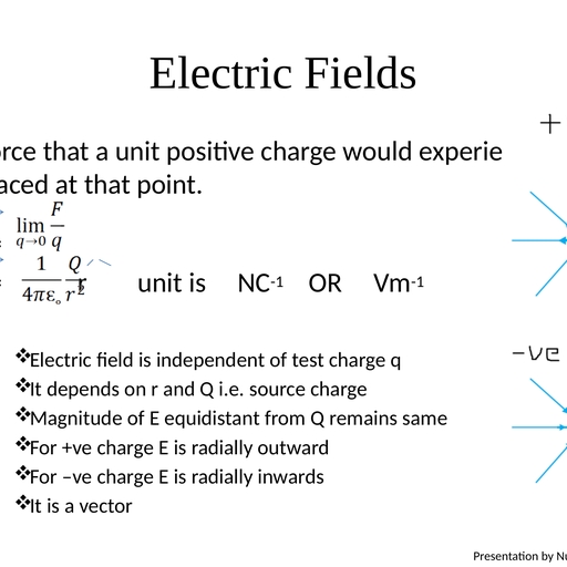
PN junction &p-n junction formation, A p-n junction is the basic building block of many, semiconductor devices like diodes, transistor, etc., the junction between p and n material is called PN junction, p-n junction formation, • Consider a thin p-type silicon (p-Si) semiconductor wafer., By adding precisely a small quantity of pentavalent, impurity, part of the p-Si wafer can be converted into n-Si., The wafer now contains p-region and n-region and a, metallurgical junction between p-, and n- region, • Two important processes occur during the formation of a pn junction:, • diffusion and drift.
Page 3 :
in p-type section holes are majority carriers and in N section, electrons are the majority carriers. due to high, concentration of different type of charge Carriers holes, from the P region diffuse into n region and electron from n, region diffuse into P region giving rise to diffusion current., • When an electron diffuses from n → p, it leaves behind an, ionised donor on n-side. This ionised donor (positive, charge) is immobile as it is bonded to the surrounding, atoms. As the electrons continue to diffuse from n → p, a, layer of positive charge (or positive space-charge region) on, n-side of the junction is developed
Page 4 :
• Similarly, when a hole diffuses from p → n due to the, concentration gradient, it leaves behind an ionised, acceptor (negative charge) which is immobile. As the, holes continue to diffuse, a layer of negative charge (or, negative space-charge region) on the p-side of the, junction is developed., • This space-charge region on either side of the junction, together is known as depletion region as the electrons, and holes taking part in the initial movement across, the junction depleted the region of its free charges, thickness is of the order of 1/10μm
Page 5 :
the loss of electron from n, region and gain of, electron from P region, causes a potential across, the junction of the two, regions. the polarity of, this is such as to oppose, the further flow of, careers This potential is, called barrier potential ., , • due to positive space, charge region on N side of, the junction and negative, space charge region on, the P side an electric field, directed from the positive, charge towards a negative, charge develops. due to, this electrons from P side, move towards the n side, and holes from the n, region to p region giving, rise to drift current
Page 6 :
Diode under equilibrium (V=0), , Barrier potential under no bias, , • the loss of electron, from n region and gain, of electron from P, region causes a, potential across the, junction of the two, regions. the polarity of, this is such as to oppose, the further flow of, careers This potential is, called barrier potential
Page 7 :
• . initially diffusion current is large and drift, current is small. as the diffusion process, continuous space charge region on either side, extends. thus increasing the electric field and, hence drift current increases. this process, continues until diffusion current equals the, drift current. Thus a PN junction is formed., under equilibrium in a PN junction net current, is zero.
Page 8 :
semic onductor diode, , Semiconductor diode,, , Symbol for p-n junction diode., , • it is a PN junction with metallic contacts, provided at the ends of the for the application, of external voltage., • biasing :- applying an external potential on, two sides of a PN junction
Page 9 :
• ., • battery is connected to the diode through rheostat so, as to vary the applied voltage and corresponding, current is noted. the current increases slowly, almost, negligibly till voltage crosses certain value., • after the characteristic voltage the diode current, increases exponentially even for a small increase in the, bias voltage., • the voltage at which current increases sharply is called, knee voltage, threshold voltage or cut in voltage
Page 10 :
p-n junction diode under forward bias, • When an external voltage V is, applied across a, semiconductor diode such that, p-side is connected to the, positive terminal of the, battery and n-side to the, negative terminal it is said to, be forward biased., • The direction of the applied, voltage (V) is opposite to the, built-in potential Vₒ. As a, result, the depletion layer, width decreases and the, barrier height is reduced The, effective barrier height under, forward bias is (V ₒ– V ).
Page 11 :
• If the applied voltage is small, the barrier potential will be reduced only slightly, below the equilibrium value, and only asmall number of carriers in the, material—those that happen to, • be in the uppermost energy levels—will possess enough energy to cross the, junction. So the current will be small., • If we increase the applied voltage significantly, the barrier height will be, reduced and more number of carriers will have the required energy. Thus the, current increases., • Due to the applied voltage, electrons from n-side cross the depletion region, and reach p-side (where they are minority carries). Similarly, holes from p-side, cross the junction and reach the n-side (where they are minority carries). This, process under forward bias is known as minority carrier injection., • At the junction boundary, on each side, the minority carrier concentration, increases significantly compared to the locations far from the junction., • Due to this concentration gradient, the injected electrons on p-side diffuse, from the junction edge of p-side to the other end of p-side. Likewise, the, injected holes on n-side diffuse from the junction edge of n-side to the other, end of n-side, • this motion of charged carriers on either side gives rise to current. The total, diode forward current is sum of hole diffusion current and conventional current, due to electron diffusion. The magnitude of this current is usually, • in mA.
Page 12 :
p-n junction diode under reverse bias, •, , •, •, , •, •, •, , •, , When an external voltage (V ) is applied, across the diode such that n-side is, positive and p-side is negative, it is said to, be reverse biased, The applied voltage mostly drops across, the depletion region., The direction of applied voltage is same as, the direction of barrier potential. As a, result, the barrier height increases and, the depletion region widens due to the, change in the electric field., The effective barrier height under reverse, bias is (Vₒ+ V ), This suppresses the flow of electrons from, n → p and holes from p → n., Thus, diffusion current, decreases, enormously compared to the diode, under forward bias.
Page 13 :
• The electric field direction of the junction is such that if electrons on pside or holes on n-side in their random motion come close to the junction,, they will be swept to its majority zone. This drift of carriers gives rise to, current. The drift current is of the order of a few μA., • This is quite low because it is due to the motion of carriers from their, minority side to their majority side, • The diode reverse current is not very much dependent on the applied, voltage. Even a small voltage is sufficient to sweep the minority carriers, from one side of the junction to the other side of the junction. The, currentis not limited by the magnitude of the applied voltage but is limited, due to the concentration of the minority carrier on either side of the, junction., • The current under reverse bias is essentially voltage independent upto a, critical reverse bias voltage, known as breakdown voltage (Vbr ). When, V = Vbr, the diode reverse current increases sharply. Even a slight increase, in the bias voltage causes large change in the current., • If the reverse current is not limited by an external circuit below the rated, value (specified by the manufacturer) the p-n junction will get destroyed.
Page 14 :
V-I characteristics of, a p-n junction diode, • The circuit arrangement for, studying the V-I characteristics, • of a diode, (i.e., the variation, of current as a function of, applied voltage) are shown in, Fig., • The battery is connected to, the diode through a, potentiometer (or reheostat), so that the applied voltage to, the diode can be changed. For, different values of voltages,, the value of the current is, noted. A graph between V, • and I is obtained as in Fig.
Page 15 :
•, , •, , •, , •, , In forward bias, the current first, increases very slowly, almost, negligibly, till the voltage across the, diode crosses a certain value., After the characteristic voltage, the, diode current increases significantly, (exponentially), even for a very small, increase in the diode bias voltage., This voltage is called the threshold, voltage or cut-in voltage (~0.2V for, germanium diode and~0.7 V for, silicon diode)., For the diode in reverse bias, the, current is very small (~μA) and, almost remains constant with change, in bias. It is called reverse saturation, current. However, for special cases, at, very high reverse bias (break down, voltage), the current suddenly, increases. The general purpose diode, are not used beyond the reverse, saturation current region.
Page 16 :
• the p-n junction diode primarily allows the, flow of current only in one direction (forward, bias). The forward bias resistance is low as, compared to the reverse bias resistance., • dynamic resistance as the ratio of small, change in voltage ∆V to a small change in, current ∆ I:
Page 17 :
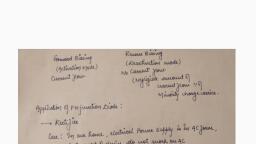
•, •, •, , •, •, •, •, •, , •, , ∆ Forward biasing, when positive terminal of a battery is connected to, Pside and and negative terminal is connected to N, side, majority charge Carriers move towards the, Junction., the direction of the applied voltage is opposite to, builtin voltage VP. effective barrier height is V - V0., height of the potential barrier and width of the, depletion layer decreases., diode offers no resistance to flow of current., large number of majority carriers cross junction, boundary., the minority carrier concentration increases, compared to the sites far from the junction. due to, this concentration gradient electrons from P side of, the junction diffuse to the other end of the p side, .similarly hole diffuse in n side, net current is sum of hole diffusion current +, electron diffusion current, , •, •, •, , •, •, •, •, •, •, , •, , Reverse biasing, when negative terminal of a battery is connected, to Pside and and positive terminal is connected to, N side, majority charge Carriers move away from the, Junction., the direction of the applied voltage is same as the, builtin voltage VP. effective barrier height is V + V0., height of the potential barrier and width of the, depletion layer increases., diode offers high resistance to flow of current., majority carriers can not cross junction boundary., some minority Carriers across the junction give rise, to reverse current., minority Carriers are drifted into the majority zone., this drift current is of the order of few A.reverse, current is independent of applied voltage.
Page 18 :
•, •, , •, •, , •, , FB characteristics, battery is connected to the diode through, rheostat so as to vary the applied voltage and, corresponding current is noted. the current, increases slowly, almost negligibly till voltage, crosses certain value., after the characteristic voltage the diode, current increases exponentially even for a, small increase in the bias voltage., the voltage at which current increases, sharply is called knee voltage, threshold, voltage or cut in voltage, , •, •, , •, •, , •, , •, , reverse bias characteristics, current is very small and almost remains the, same with the change in the Voltage, till, certain voltage called reverse saturation, current ., as the reverse bias increases the current, increases suddenly at certain voltage ., the maximum reverse, potential difference which a diode can, withstand without breakdown is called, reverse breakdown voltage or Zener voltage., it is characteristic of pn junction., (as reverse voltage increases the covalent, bonds are broken and large number of, electron hole pairs are produced hence the, current increases sharply
 Learn better on this topic