Notes of 12th(Science), Physics Chapter 16.pdf - Study Material
Page 1 :
*Saraswati, , IMP Pocket Study * Std. XII : PHYSICS, , 1, , Chapter No. 16, , Semiconductor Devices, Summary :, A semiconductor device is an electronic components, that relies on the electronic properties of a, semiconductor material (primarily Silicon (Si),, germanium (Ge) and gallium (Ga), arsenide (As) as, well as organic semiconductors) for it's function., In this chapter we will study about the semiconductor, devices - a conductor made with semiconducting, material., Semiconductor types like n type and p type are, studied as well as semiconductor diodes e.g. zener, diode, P.N. junction diode. Photodiode, LED, Solar Cell,, Photovoltaic cell as well as rectilier like full wave and, half wave rectifter., In this chapter we will study about Transistor which, acts as a switch, as an amplifier., Logic gate is a digital circuit which produces definite, output (high or low) for given input (high or low), combination e.g. AND, OR, NOT, NAND and NOR, with truth table & Boolean expression for it.
Page 2 :
*Saraswati, , IMP Pocket Study * Std. XII : PHYSICS, , 2, , : EXERCISES :, Q.1Choose the correct options., i) In a BJT, largest current flows occurs., (a) In the emitter, (b) In the coollector, (c) In the base, (d) Through CB junction, ii) A series resistance is connected in the zener, diode circuit to ................, (a) Properly forward bias the zener, (b) Protect the zener, (c) Properly forward bais the zener, (d) Protect the load resistance, iii) A LED emits visible light when its............., (a) Junction is reverge biased, (b) Decletion region widens, (c) Holes and electrons recombine, (d) Junction becomes hot, iv) Solar cell operates on the principle ............., (a) Diffusion, (b) Recombination, (c) Photo voltaic action (d) Carrier flow
Page 3 :
*Saraswati, , v), (a), (b), (c), (d), , IMP Pocket Study * Std. XII : PHYSICS, , 3, , A logic gate is an electronic circuit which............, Makes logical decisions, Allows electron flow only in one direction, Work using binary algebra, alternates between O and 1 value, , Ans : i) - (a) In the emitter, ii) - (b) Protect the zener,, iii) - (c) Holes and electrons recombine, iv) - (c) Photo, voltaic action, v) - (d) alternates between O and 1 value, Q.2. Answer in brief., i) Why is the base of a transistor made thin and, is lightly doped?, Ans : i) The base region is thin so that the majority charge, carriers coming from emitter find themselves near the, base collector juction and move to collector instead of, going to base terminal., ii) It is lightly dopped so that the depletion region is, thin, electric field is strong and the resistance is small, ii) How is a zener diode different than an, ordinary diode ?, Ans : i) Zener diode is a spceical purpose semiconductor
Page 4 :
*Saraswati, , IMP Pocket Study * Std. XII : PHYSICS, , 4, , diode works on the principle of junction breakdown where, as other diodes make use of photo sensitivty., ii) Zener diode is a voltage regulator., iii) Protector against meter damage from accidental, fluctuations., iii) On which factors does the wavelength of light, emitted by a LED depend ?, Ans : The wavelength of light emitted by a LED depends, on following factors:i) LEDs are fabricated by using compound, semiconductors made with elements such as Gallium., Phosphorus and Arsenic, by varying the proportions of, these elements in the semiconductor., ii) Forward current value., iv) Why should a photodiode be operated in, reverse biased mode?, Ans : Because only minority current flows throught a, photodiode. The reverse current depends only on the, concentration of the minority carriers and not on the applied, voltage. The reverse current of a photodiode depends on, the intensity of the incident light.
Page 5 :
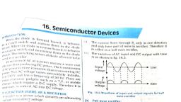
*Saraswati, , IMP Pocket Study * Std. XII : PHYSICS, , 5, , v) State the principle and uses of a solar cell., Ans : Principle : Light incident an a solar cell produces, both a current and a voltage to generate electric power, (Sourse of DC power), Uses : i) Supply power for electric equipment at a, remote place on earth or abord a sattelite or a space, station., ii) Charging batteries of day time so that these are, used in night., iii) To supply power to traffic signals in communication, stations, calculation, iv) Lux meter to measure intensity of light., Q.3. Draw the circuit diagram of a halfwave rectifier., Explain its working. What is the frequency of ripple, in its output?, Ans : Circuit diagram of half wave rectifier.
Page 6 :
*Saraswati, , IMP Pocket Study * Std. XII : PHYSICS, , 6, , Working of half wave rectifier :, i) The AC voltage across the secondary coil A B, changes it’s polarities after every half cycle., ii) When positive half cycle begins, the voltage at the, point A is at higher potential with respect to that at, point B, therefore the diode D is forward biased. It, conducts as current flows through the circuit works as a, closed switch., iii) When the negative half cycle begins, the potential, at A is lower with respect to point B and the diode is, is reverse biassed, therefore, it does not conduct (works, as open switch) No current passed through the, circuit., iv) Hence, the diode conducts only in the positive half, cycle of the AC input and it blocks the current during the, negative half cycle., Waveforims for input and output voltage :
Page 7 :
IMP Pocket Study * Std. XII : PHYSICS 7, i) Current always flows throught the load RL in the, same direction for a alternating positive half cycles., Hence, DC output voltage obtained across RL in the form, of alternate palses., ii) The output frequeny is 50 Hz because for one AC, input pulsating we get one cycle of DC., *Saraswati, , Q.4. Why do we need filters in a power supply?, Ans : We need filters in a power supply because:i) A filter circuit is used to remove the ripple from the, output of a rectifier., ii) It is useful to removes the AC component or the, ripple from a rectifier output and allows only the DC, component., Q.5. Draw a neat diagram of a full wave rectifier and, explain it’s working?, Ans : Circuit diagram for full wave rectifier
Page 8 :
*Saraswati, , IMP Pocket Study * Std. XII : PHYSICS, , 8, , Working :, i) The circuit consists of a centre tapped fransforme, and diodes, D1 & D2, ii) The diodes D1&D2 are connected such D1 conducts, in the positive half cycle and D2 Conducts in the negative, half cycle of the input voltage., iii) During the positive half cycle of the input voltage., The point A is at a higher potential than that of the, the point B and the diode D1 conduits the current through, load resistance RL (across APQRS)., iv) During the negative half cycle of the input voltage, point B is at higher potential than point A and diode D2, conducts, the current throught load resistance RL (across, BPQRC)., Wave forms of inpunt and output voltages :
Page 9 :
*Saraswati, , IMP Pocket Study * Std. XII : PHYSICS, , 9, , Thus the current flowing through the load, resistance is in the same direction both the cycles., The outpur frequency is 100 Hz because for input, AC cycle we get two cycles of pulsating DC, Q.6. Explain how a zener diode maintains constant, voltage across a load?, Ans :, , i) The circiut diagram of zener diode as voltage, regulator across load RL connected in parallel with zener, diode V0 VZ . The output voltage Vo is taken across, , RL, , , , , , ii) When voltage is applied to the circuit, current I, flows through it. I is divided into I z and I l where
Page 10 :
*Saraswati, , IMP Pocket Study * Std. XII : PHYSICS, , 10, , I Z current through zener diode and, I L current through R L, from fig. I Iz I L, , Vi Vs VZ, Vi IRs Vz, , But, , V IR, , I , , I z I L , Vi I z I L Rs Vz, Vi I z I L Rs Vo, , VZ VO, , iii) If input voltage Vi is increased beyond zener, voltage. I increases such that current I Z through zener, diode increases but I L - Current through RL remains same., Therefore V0 output voltage across load resistance, remains the same., iv) If input voltage Vi is decreased beyond zener, voltage. I decreases such that current I Z through zener, diode decreases but current I L through RL remains same., Therefore output voltage across load resistance remains, same., v) So zener diode acts as a voltage regulator. once, the breakdown voltage is observed it remains constant, though current is increased.
Page 11 :
*Saraswati, , IMP Pocket Study * Std. XII : PHYSICS, , 11, , Q.7. Explain the forward and the reverse, characteristic of a zener diode?, Ans : Forward and reverse characteristic of zoner diode, is a shown in the fig., , fig. : IV Characteris curve for zener diode
Page 12 :
*Saraswati, , IMP Pocket Study * Std. XII : PHYSICS, , 12, , Forword Characteristics :, i) A-Zener diode behaves like a normal diode, ii) In forword bias, as zener voltage VF increases, current increases initially in small amout upto the value, 0.3V to 0.7V of voltage., iii) After this voltage current increases suddently, having it’s maximum value of forward current I F, Reverse Characteristics :, i) When it is in reverse bias mode, it shows, breakdown. Which occurs at a voltage called zener voltage, , VZ, ii) The current suddently increases if the applied, voltage is increased beyond the zener voltage., iii) Voltage remain constant at VZ , for increasing, current, once the zener breakdown occurs., iv) This property of the zener diode is used in a voltage, regulator. VZ depends upon amount of doping., Q.8. Explain the working of a LED :Ans :
Page 13 :
*Saraswati, , IMP Pocket Study * Std. XII : PHYSICS, , 13, , i) Fig. shows the emission of light whe electron hole, pair combines., ii) When the diode is in forword biased, electrons, from the semiconductors conduction band recombine with, holes from the valence band releasing sufficient energy, to produce photons which emit a monochromatic, light., iii) Because of a thin layer, a reasonable number of, these photons can leave the junction and emit coloured, light, iv) the amount of light output is directly proportional, to the forward current. Thus higher the forward current, higher is the light output.
Page 14 :
IMP Pocket Study * Std. XII : PHYSICS 14, The intensity of emitted light :, i) The colour of emitted light depends upon band, gap of the material used., ii) Different compound semiconductor are used to get, LEDs of different colours., e.g., a) Ga - As LED emits infra-red light, b) Ga - As - P LED emits red and yellow light, c) Ga - P LED emits red, green light, *Saraswati, , Q.9. Explain the construction and working of solar, cell., Ans :, , i) It consists of a p.n juction, ii) The n-side of the juction faces the solar radiation
Page 15 :
IMP Pocket Study * Std. XII : PHYSICS 15, iii) the p-side is relatively thick and is at the back of, the solar cell, iv) Both p and n-side one coated with a conducting, material, v) The n-side is coated with antireflection coating, which allows visible light to pass through it, vi) The main function of this coating is to reflect the, IR radiations and protect the solar cell from heat, vii) The coating works as electrical contact in which, n-side coating is front contact and p-side coating is, back or rear contact, Working:i) While junction is formaing depletion layer and, potential barrier builds up because of crossing of majority, carriers accross the junction, ii) When photons of energy greater than band gap, hv, Eg are incident on the cell, the photons are, absorbed and electron hole pairs are generated, iii) The barrier potential segregates them and pushes, electrons to N side and holes to P side, iv) The displacement of charges set up potential, difference across two regions with p-side as positive and, n-side as negative electrode, v) If external load RL is connected current I flows, *Saraswati
Page 16 :
*Saraswati, , IMP Pocket Study * Std. XII : PHYSICS, , 16, , through it and we get electrical energy, vi) A solar cell can generate photo voltage in the, range of 0.5V to 1.2V, Q.10 Explain the principle of operaation of a, photodiode., Ans : When a p-n juction diode is reverse biased a, reverse saturation current flows throught the junction. The, magnitude of this current is constant for a certain range, of reverse bias voltage. This current is due to the minority, carriers on either side. This current is called dark current, in a photodiode because if flows even when the photodiode, is not illumunated., , i) When a pn junction is illuminated electron hole, pairs are generated in the depletion region., ii) The energy of the incident photons should be larger
Page 17 :
IMP Pocket Study * Std. XII : PHYSICS 17, than the band gap of the semiconductor material used, to fabricate the photodiode., iii) The electrons and the holes are separated due to, the intrinsic electric field present in the depletion region, iv) The electrons are attracted towards the anode, and the holes are attracted towards the cathode., v) More carriers are available for conduction and, reverse current is increased., vi) The reverse current of a photodiode depends on, the incident light. Thus reverse current can be controlled, by controlling the concentration of minority carriers in the, junction., *Saraswati, , Q.11 What do you mean by a logic gates, a truth, table and a Boolean expression?, Ans : Logic gate : A digital circuit with one or more, input signals but only one output signal is called a logic, gate., It is a switching circuit that follows certain logical, relationship between the input and output voltages,, therefore they are generally known as logic gates, because, they control the flow of signal or information., Truth Table : Each logic gate is indicated by symbol, and its function is defined by a truth table which shows all
Page 18 :
*Saraswati, , IMP Pocket Study * Std. XII : PHYSICS, , 18, , possible combinations of the input and corresponding, outputs., Boolean Expression : The mathematical statement, that provid the relationship between the input and output, of a logic gate is called a Boolean Expression., Q.12 What is logic gate? Write down truth table, and a boolean expression for AND gate?, Ans : Logic gate : A digital circuit with one or more input, signals but only one output signal is called as a logic gate., Truth table for AND gate, , Input A Input B, Output Y, 0, 0, 0, 0, 1, 0, 1, 0, 0, 1, 1, 1, Boolean expression for AND gate, , Y A.B
Page 19 :
IMP Pocket Study * Std. XII : PHYSICS 19, Q.13 What are the uses of logic gates? Why is a, NOT gate known as an inverter?, Ans : Uses of logic gates :, i) All logic gates are basic building blocks of all digital, systems., ii) Basic gates are used to construct NAND and, NOR gates., iii) NAND and NOR gates are universal building, blocks to construct digital circuits used in digital clocks,, computers etc., iv) Gates are used in boolean algebra., v) The binary arith matic operations, such as addition,, multiplication etc can be realised through logic gates A, NOT gate producs high output when its input is low. It, produces low output where its input is high, so that a NOT, gate acts as an ‘Inverter gate’., *Saraswati, , Q.14. Write teh Boolean expression for (i) OR gate, (ii) AND gate (iii) NAND gates?, Ans : Boolean Expressions for:i) OR Gate Y A B, ii) AND gate Y A . B, iii) NAND gate Y A . B
Page 20 :
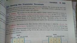
*Saraswati, , IMP Pocket Study * Std. XII : PHYSICS, , 20, , Q.15 Why is the emitter, the base and the collector, of a BJT dopped differently?, Ans : Emitter : It is a thick heavily doped layer. Thus, supplies a large number of majority carriers for the current, flow through the transistor., Base : It is a thin, lightly dopped central layer., Collector : It is on the other side of the base. It is, also thick and moderately doped layer. It’s area is larger, than, that of the emitter and the base. This layer collects, a major portion of the majority carriers supplied by the, emitter. The collector also help dissipation of any small, amount of heat generated, so that base, emitter and, collector of a BJT dopped differently., Q.16 Which method of biasing is used for operating, transistor as an amplifier?, Ans : Irrespective fo configuration (common base,, common emitter or common collector) the emitter of, transistor is forward biased and collectr is reverse blased,, so transistor as an amplifier, Q.17 Define and . Define or derive relation, between them., Ans : i) D.C common base current gain dc :, ,
Page 21 :
*Saraswati, , IMP Pocket Study * Std. XII : PHYSICS, , 21, , It is defined as the ratio of collector current to, emitter current. dc , , IC, IE, , ii) D.C common emitter current gain, , :, dc, , It is defined as the ratio of collector current to, emitter current. dc , , IC, IB, , iii) Relation between dc & dc :, Since I E I B I C dividing throughout by I C ,, we have, , I E I B IC, , , IC IC IC, , , , 1, 1, , 1, dc dc, , , , dc dc (i ), , 1 dc , , dc , (ii), dc , , 1dc , Equations i) and ii) represent the required relation, between d c and dc ( ), ,
Page 22 :
*Saraswati, , IMP Pocket Study * Std. XII : PHYSICS, , 22, , Q.18. The common base DC current gain of a, transistor is 0.967. If the emitter current is 10 mA., What is the value of base current?, Ans : Given : dc 0.967, , I E 10 mA 10 10-3 A, To find : I R ?, Solution : I C dc I E, , , , 0.967 10 10 3, I C 0.967 10 3, I B I E IC, 10 103 A 9.67 103 A, I B 0.33 10 3 A, I B 0.33mA, , Or, The value of base current is 0.33mA., , Q.19 In a common base connection, a certain, transistor has an emitter current of 10mA and, collector current of 9.8 mA. Calculate the value of, the base current?, Ans : Given :, I E 10mA, , I C 9.8mA
Page 23 :
*Saraswati, , IMP Pocket Study * Std. XII : PHYSICS, , To find :, , 23, , IB ?, , Solution : dc , , IC, IE, , 98, 10, dc 0.98, , , dc , but, , dc, 0 .9 8, , 49, 1 d c 1 0 .9 8, , IC, IB, I, 9.8, IB C , mA, dc 49, I B 0.2mA, , dc , , The value of base current is 0.2mA., Q.20 In a commun base connection, the emitted, current is 6.28 mA and a collector current is 6.20mA., Determine the common base DC current gain?, Ans : Given :, , I E 6.28mA
Page 24 :
*Saraswati, , IMP Pocket Study * Std. XII : PHYSICS, , 24, , I C 6.20mA, To find : dc ?, , IC, Solution : dc I, E, , , , 6.20mA, 6.28mA, , dc 0.987, The common base DC current gain = 0.987
 Learn better on this topic