Notes of Msc Sem 4 Microprocessor, Microprocessor 8085 notes sem 4s.pdf - Study Material
Page 2 :
INDEX, CHAPTER 1, 1.1, 1.2, 1.3, 1.4, 1.5, 1.6, , Introduction to Microprocessor, Microprocessor architecture and its operations, Memory, Input & output devices, Logic devices for interfacing, The 8085 MPU, Example of an 8085 based computer, Memory interfacing, , 2.1, 2.2, 2.3, 2.4, 2.5, 2.6, 2.7, 2.8, 2.9, 2.10, 2.11, , CHAPTER 2, Basic interfacing concepts, Interfacing output displays, Interfacing input devices, Memory mapped I/O, Flow chart symbols, Data Transfer operations, Arithmetic operations, Logic Operations, Branch operation, Writing assembly language programs, Programming techniques: looping, counting and indexing, , 3.1, 3.2, 3.3, 3.4, 3.5, 3.5.1, 3.5.2, 3.5.3, 3.5.4, 3.6, 3.7, 3.8, 3.9, 3.9.1, , CHAPTER 3, Additional data transfer and 16 bit arithmetic instruction, Arithmetic operations related to memory, Logic operation: rotate, compare, Counter and time delays, Illustrative program, Hexadecimal counter, zero-to-nine, (module ten) counter, Generating pulse waveforms, Debugging counter and time delay, Stack, Subroutine, Restart, Conditional call and return instructions, Advance subroutine concepts, The 8085 Interrupts, 8085 vector interrupts., , CHAPTER 4, , 3
Page 3 :
4.1, 4.2, 4.3, 4.4, 4.5, 4.6, 4.7, , BCD-to-Binary conversion, Binary-to-BCD conversion, BCD-to-Seven segment code converter, Binary-to-ASCII, ASCII-to-Binary code conversion, BCD Addition, BCD Subtraction, , 4.8, 4.9, , Introduction to Advance instructions and Application, Multiplication, Subtraction with carry, , 5.1, 5.2, 5.3, 5.4, 5.5, 5.6, 5.7, , CHAPTER 5, 8255 Programmable peripheral interface, interfacing keyboard and seven segment display,, 8254 (8253) programmable interval timer,, 8259A programmable interrupt controller,, Direct Memory Access and 8237 DMA controller., Introduction to 8086 microprocessor: Architecture of 8086, Pin diagram, Functional block diagram, Register organization., , 3
Page 4 :
UNIT 1, 1.1, INTRODUCTION TO MICROPROCESSOR: Microprocessors are regarded as, one of the most important devices in our everyday machines called computers. Before we start, we, need to understand what exactly microprocessors are and their appropriate implementations., Microprocessor is an electronic circuit that functions as the central processing unit (CPU) of a, computer, providing computational control. Microprocessors are also used in other advanced, electronic systems, such as computer printers, automobiles, and jet airliners Typical microprocessors, incorporate arithmetic and logic functional units as well as the associated control logic, instruction, processing circuitry, and a portion of the memory hierarchy. Portions of the interface logic for the, input/output (I/O) and memory subsystems may also be infused, allowing cheaper overall systems., While many microprocessors and single-chip designs, some high- performance designs rely on a few, chips to provide multiple functional units and relatively large caches. When combined with other, integrated circuits that provide storage for data and programs, often on a single semiconductor base, to form a chip, the microprocessor becomes the heart of a small computer, or microcomputer., Microprocessors are classified by the semiconductor technology of their design (TTL, transistortransistor logic; CMOS, complementary-metal-oxide semiconductor; or ECL, emitter-coupled logic),, by the width of the data format (4-bit, 8-bit, 16-bit, 32-bit, or 64-bit) they process; and by their, instruction set (CISC, complex-instruction-set computer, or RISC, reduced-instruction-set computer;, see RISC processor). TTL technology is most commonly used, while CMOS is preferred for portable, computers and other battery-powered devices because of its low power consumption. ECL is used, where the need for its greater speed offsets the fact that it consumes the most power. Four-bit devices,, while inexpensive, are good only for simple control applications; in general, the wider the data format,, the faster and more expensive the device. CISC processors, which have 70 to several hundred, instructions, are easier to program than RISC processors, but are slower and more expensive., Microprocessors have been described in many different ways. They have been compared with the, brain and the heart of humans. Their operation has been likened to a switched board, and to the, nervous system in an animal. They have often been called microcomputers. The original purpose of, the microprocessor was to control memory. That is what they were originally designed to do, and, that is what they do today. Specifically, a microprocessor is “a component that implements memory., A microprocessor can do any information-processing task that can be expressed, precisely, as a plan., It is totally uncommitted as to what its plan will be. It is a truly general-purpose informationprocessing device. The plan, which it is to execute—which will, in other words, control its, operation—is stored electronically. This is the principle of “stored program control”. Without a, program the microprocessor can do nothing. With one, it can do anything. Furthermore,, microprocessors can only perform information-processing tasks. To take action on the outside, world, or to receive signals from it, a connection must be provided between the microprocessor’s, representation of information (as digital electronic signals) and the real world representation., 4-BIT MICROPROCESSORS:, Historically, the 4-bit microprocessor was the first general-purpose microprocessor introduced on the, market. The basic design of the early microprocessors was derived from that of the desk
Page 5 :
calculator. The Intel 4004, a 4-bit design, was t4he grandfather of microprocessors. Introduced in, late 1971, the 4004 was originally designed for a Japanese manufacturer as the processing element of, a desk calculator; it was not designed as a general-purpose computer. The shortcomings of the 4004, were recognized as soon as it was introduced. But it was the first general-purpose computing device, on a chip to be placed on the market. Many of the chips introduced at about the same time by other, companies were, in fact, mere calculator chips. Some of them were even serial-by-bit devices, which, performed calculations a single bit at a time. The Intel 4004 chip took the integrated circuit down, one step further by placing all the parts that made a computer think (i.e. central processing unit,, memory, input and output controls) on one small chip. Programming intelligence into inanimate, objects had now become possible. The 4004 was the world's first universal microprocessor. In the, late 1960s, many scientists had discussed the possibility of a computer on a chip, but nearly everyone, felt that integrated circuit technology was not yet ready to support such a chip. Intel's Ted Hoff felt, differently; he was the first person to recognize that the new silicon-gated MOS technology might, make a single-chip CPU (central processing unit) possible., , 8-BIT MICROPROCESSORS:, Today, 8-bit microprocessors coexist with 16-bit microprocessors as the design standard. Although 16bit chips provide higher performance computationally, 8-bit designs have more than adequate power, for many applications—plus the advantage of lower cost. As originally design, most 16-bit, microprocessors were limited to packages with a maximum of 40 to48 pins. This was not due to, physical, but rather to economic, constraints: industrial tester of the time was generally limited to 40pin DIPs. The ancestor of today’s 8-bit microprocessors was the Intel 8008, introduced in 1972- 1973., The 8008 was not intended to be a general-purpose microprocessor. IT was to be a CRT display, controller for Data point. Taking into account all of its design inadequacies and its limited, performance, the 8008 was an overwhelming success. (Bernstein, p.202), INTEL (8-BIT MICROPROCESSORS) :, The 8080, designed as a successor to Intel’s 8008, was the first powerful microprocessor introduced, on the market. Several other microprocessors of similar performance were introduced on the market, within a year after the 8080 appeared, and several additional powerful designs were introduced later., Technically, however, the 8080 long remained the most powerful product on the market., Furthermore, Intel was the first company to invest in the development of support chips and software, for its products. This ensured the continued success of the 8080 because its performance was then, sufficient for many applications. The early 8080 competitors were introduced with at least a ninemonth delay and failed to dislodge it. The 8080 is still sold today thought It has been largely eclipsed, by successor products—most notably the 8085 microprocessor. Today, the 8085 accounts for roughly, one of every four 8-bit microprocessors sold., 1.2, MICROPROCESSOR ARCHITECTURE AND ITS OPERATION:, Computer system consist primary of :1- Microprocessor., 2-Memory., 3-Input., 4-Output., The internal logic design of the microprocessor called its"architecture", determine how and, what various operations are performed by "MICROPROCESSOR"., Microprocessor architecture and its operations: The microprocessor is programmable logic, device designed with register,flip-flop and timing elements., All function performed by microprocessor can by classified in three general categories:-1-
Page 6 :
Microprocessor initiated operations., 2- Internal data operations., 3- Peripheral (or externally) initiated operations., To performed these operations, microprocessor needs [logic circuit and control signals]., 1- Microprocessor Initiated Operations:Primarily microprocessor performs four operations:a) Memory read (Reads data from memory)., b) Memory writes (Write data into memory)., c) I/O read (Accept data to output device)., d) I/O writes (Sends data to output device)., These operation are part of communication process., Microprocessor performed these functions using sets of buses [Data bus, Address bus, Control, bus]., Data bus: - is a group of 8 lines used for data flow, these lines are bidirectional from (00 – FF) =28, =256 numbers. The largest number = 1111 1111 = FF , thus 8085 Microprocessor is called 8bit, Microprocessor., Address bus: - is a group of 16 lines, identified as 0 – 15. This bus is unidirectional (bit flow in, one direction) from Microprocessor to peripheral. Each memory location or peripheral identified, with binary number called address. (216 =65536=64K)., Control bus: - the control is comprised of various single lines that carry synchronization signals., , Fig. 1.1 The 8085 Bus System, The microprocessor needs to perform the followingsteps:i) Identify the peripheral (memory location)., ii) Transfer data., iii) Provide timing or synchronization signals., 2- Internal Data Operations:The internal architecture of the 8085/8080A microprocessor determines how and what operation can, be performed with the data. These operations are:-
Page 7 :
Store 8-bit data., , Performed arithmetic and logical operations. Test for conditions.Sequence the, , execution of instructions. Store data temporarily during execution in the defined R/W memory, locations called the stack.To perform these operations the Microprocessor requires:a) Registers., b) An arithmetic logic unit (ALU) & control logic., c) Internal buses (paths for information flow)., Fig1.2 : The 8085 Programmable Register, , 3- Peripheral or Externally Initiated Operations:External devices (or signals) can initiate the following operation for which individual pins on, Microprocessor chip are assigned: Reset, Interrupt, Ready, Hold., A), Reset: when reset is activated all internal operations are suspended and the program counter, iscleared., B), Interrupt: the Microprocessor can be interrupted from normal execution and asked to, execute other instructions called "service routine" (emergency), Microprocessor resumes its, operation after that., C), Ready: 8085 has pin called ready, if the signal is low Microprocessor enters into wait state,, thissignal used to synchronized slower peripherals with Microprocessor., D), Hold: when hold pin activated by external signal Microprocessor relinquishes control buses, and allows the external peripheral to use the. For example: Hold signal is used in direct memory, accessdata transfer., 1.3, MEMORY, INPUT AND OUTPUT: Memory is an essential component of a, microprocessor system; it stores binary information. The memory is made up of semiconductor, material used to store the programs and data. The types of memory is, Primary or main memory and, Secondary memory., Primary memory: RAM and ROM are examples of this type of memory. Microprocessor uses it in, storing a program temporarily (commonly called loading) and executing a program. Hence the speed, of this type of memory should be fast.
Page 8 :
Secondary memory: These are used for bulk storage of data and information. The main examples, include Floppy, Hard Disk, CD-ROM, Magnetic Tape etc. Slower and Sequential Access, Nature.non-volatile nature., , Fig. 1.3 Memory chip, The Basic Memory Element: The basic memory element is similar to a D latch.This latch has an, input where the data comes in. It has an enable input and an output on which data comes out., , Fig. 1.4 D Latch, , Fig.1.5: D latch as a 4-bit storage element, Address Decoding and Memory Mapping: Memory address decoding is nothing but to assign an, address for each location in the memory chip. The data stored in the memory is accessed by
Page 9 :
specifying its address. Memory address can be decoded in two ways:, i)Absolute or Fully decoding and ii) Linear Select or Partial decodingThere are many advantages in, absolute address decoding., i), ii), , Each memory location has only one address, there is no duplication in the address, Memory can be placed contiguously in the address space of the microprocessor., i) Future expansion can be made easily without disturbing the existing circuitryThere are few, disadvantages in this method., Extra decoders are necessary, ii) Some delay will be produced by these extra decoders., The main advantage of linear select decoding is its simplified decoding circuit.This reduces the, hardware design cost. But there are many disadvantages in this decoding., i) Multiple addresses are provided for the same location, ii) Complete memory space of the microprocessor is not efficiently used, iii) Adding or interfacing ICs with already existing circuitry is difficult., Absolute Address Decoding: The 8085 microprocessor has 16 address lines. Therefore it can access 216, locations in the physical memory. If all these lines are connected to a single memory device, it will, decode these 16 address lines internally and produces 216 different addresses from 0000H to FFFFH, so that each location in the memory will have a unique address., , Fig. 1.6 Memory Address, Above diagram shows the various memory addresses used in Microprocessor. If more than one chips, are used then some logic must be used to select one particular chip. This is done with the help of, decoder., 74LS138 address decoder to generate the chip select signals for eachmemory block. In this decoder, when the address lines A13, A14 and A15 are 000, theoutput lineY0 will be activated as shown in Fig, 1.7. This in turn selects the firstmemory block. Similarly when these lines are 001 (C=0, B=0 and, A=1) Y1 will beactivated and the second memory block will be selected.
Page 10 :
Fig 1.7: Memory block decoder, In this type of memory interfacing, all the address lines (A0 to A15) have beenused. Each location in, the memory will have a single address. This type of addressdecoding is called as absolute or fully, decoded addressing., , Fig. 1.8: Role of CS signal, According to the value of Ao and A1 , any one register will be selected and to select one memory, chip we need one chip select signal CS signal as shown in the next diagram., If CS’ is ‘0’memory 1 will be selected else memory2 will be selected. And the complete picture of the
Page 11 :
interfacing is shown below. Fig. 1.9: The complete interfacing diagram, The simple view of RAM is that it is made up of registers that are made up of flip-flops (or memory, elements). The number of flip-flops in a “memory register” determines the size of the memory, word.ROM on the other hand uses diodes instead of the flip-flops to permanently hold the, information. For the microprocessor to access (Read or Write) information in memory (RAM or, ROM), it needs to do the following:, Select the right memory chip (using part of the address bus). Identify the memory location (using the, rest of the address bus). Access the data (using the data bus)., , Fig. 1.10 Memory Interface Diagram, Tri-State Buffers: An important circuit element that is used extensively in memory. This buffer is a, logic circuit that has three states: Logic 0, logic1, and high impedance. When this circuit is in high, impedance mode it looks as if it is disconnected from the output completely. This circuit has two, inputs and one output. The first input behaves like the normal input for the circuit. The second input is, an “enable”. If it is set high, the output follows the proper circuit behaviour. If it is set low, the output, looks like a wire connected to nothing., Input /Output Devices: Parallel Interfacing: There are two ways to interface 8085 with I/O devices, in parallel data transfer mode: Memory Mapped IO and IO mapped IO., Memory mapped I/O: It considers them like any other memory location. They are assigned a 16-bit, address within the address range of the 8085.The exchange of data with these devices follows the, transfer of data with memory. The user uses the same instructions used for memory., I/O mapped I/O: It treats them separately from memory: I/O devices are assigned a “port number”, within the 8-bit address range of 00H to FFH. The user in this case would access these devices using, the IN and OUT instructions only.
Page 12 :
IO mapped IO V/s Memory Mapped IO:, , Memory Mapped IO, , IO mapped IO, , •, , IO is treated as memory., , •, , IO is treated IO., , •, , 16-bit addressing., , •, , 8- bit addressing., , •, , More Decoder Hardware., , •, , Less Decoder Hardware., , •, , Can address 216=64k locations., , •, , Can address 28=256 locations., , •, , Less memory is available., , •, , Whole memory address space is available., , •, , Memory Instructions are used., , •, , Special Instructions are used like IN, OUT., , •, , Memory control signals are used., , •, , Special control signals are used., , •, , Arithmetic and logic operations can be, performed on data., , •, , Arithmetic and logic operations cannot be, performed on data., , •, , Data transfer b/w register and IO., , •, , Data transfer b/w accumulator and IO., , 1.4, LOGIC DEVICES FOR INTERFACING: Several types of interfacing devices are, necessary to interconnect the components of a bus oriented system. Tristate logic devices are, essential to proper functioning of bus oriented system., Tri state Devices: A tri state (bus driver) device is a device that can be active low, active high, or, floating. The use of a tri state device is that several of them can be connected to a single bus line, and, so long as only one of them is non-floating, the bus line can be driven by multiple senders. The, data bus is most often implemented with tri state drivers., , Fig.1.11 Tri state device, The data will be passed to the output terminal whenever the OE terminal is activated, else the device, will be in high impedance state.
Page 13 :
Fig.1.12 Octal 3 state Buffer, It is common to use an octal 3-state buffer as shown in fig. 1.12 to create a byte-wide input port. The, ‘541 has dual active-low enable inputs in order to pass its D inputs from input devices to their, respective Q outputs and onto the system data bus. OE1 could connect to the address decoder for, this input port while OE2 could connect to an active-low READ strobe. This READ strobe, requirement is imperative so as to keep the output drivers disabled and avoid the dreaded “self, destruct state” due to bus contention. Bus contention is the result of more than a single driver on a, shared bus line being active at the same time and potentially driving a bus line to opposing logic, levels. Such would be the case if the READ strobe were ignored during a CPU write operation., Bidirectional Ports: The octal bus transceivers are designed for asynchronous two-way, communication between data buses. The control-function implementation minimizes external timing, requirements., The devices allow data transmission from the A bus to the B bus or from the B bus to the A bus,, depending on the logic level at the direction-control (DIR) input. The output-enable (OE)\ input can, disable the device so that the buses are effectively isolated., Features, , , 3-State Outputs Drive Bus Lines Directly, , , , PNP Inputs Reduce dc Loading on Bus Lines, , , , Hysteresis at Bus Inputs Improves Noise Margins, , , , Typical Propagation Delay Times Port to Port, 8 ns, IC used for this purpose is 74LS245 and the pin diagram is shown below:
Page 14 :
Fig. 1.13 Logic diagram and function Table of 74LS245 Bidirectional buffer, D-Latch: Latch and flip flop are the most common logic devices that are used to store one bit data. A, simple latch has two stable logic states. The latch maintains its states indefinitely until an input pulse, called a trigger is received. If a trigger is received, the latch outputs change states according to, defined rules, and remain in those states until another trigger is received. Latches can be, interconnected to form more sophisticated circuits that function in memory chips, and microprocessors., An octal latch can hold onto the data at its inputs before transmitting the data to its outputs. This, ability is useful in applications where a number of devices share a single data bus, because it allows the, processor to store data, go onto other operations that require the bus, and return to the stored data, later if the need arises., And the group of latch or flip flop is known as register. Commonly used IC is 74LS373. Pin diagram, is shown below., Fig1.14 Pin Diagram of 74LS373
Page 15 :
1.5, 8085 MPU: The microprocessor is a semiconductor device (Integrated Circuit), manufactured by the VLSI (VeryLarge Scale Integration) technique. It includes the ALU, register, arrays and control circuit on asingle chip. To perform a function or useful task we have to form a, system by using microprocessor as a CPU and interfacing memory, input and output devices to it. A, system designed using a microprocessor as its CPU is called a microcomputer. The Microprocessor, based system (single board microcomputer) consists of microprocessor as CPU, semiconductor, memories like EPROM and RAM, input device, output device and interfacing devices. The, memories, input device, output device and interfacing devices are called peripherals. The popular, input devices are keyboard and floppy disk and the output devices are printer, LED/LCD displays, CRT, monitor, etc, The main features of 8085 μp are:, •, It is a 8 bit microprocessor., •, it is manufactured with N-MOS technology., •, It has 16-bit address bus and hence can address up to 216 = 65536 bytes (64KB) memory, locationsthrough A0-A15, • The first 8 lines of address bus and 8 lines of data bus are multiplexed AD0 – AD7, • Data bus is a group of 8 lines D0 – D7, • It supports external interrupt request. ., • A 16 bit program counter (PC), • A 16 bit stack pointer (SP), • Six 8-bit general purpose register arranged in pairs: BC, DE, HL., • It requires a signal +5V power supply and operates at 3.2 MHZ single phase clock., • It is enclosed with 40 pins DIP (Dual in line package).
Page 16 :
Fig.1.15 Pin diagram of 8085 Microprocessor, System Bus: Typical system uses a number of busses, collection of wires, which transmit binary, numbers, one bit per wire. A typical microprocessor communicates with memory and other devices, (input and output) using three busses: Address Bus, Data Bus and Control Bus., Address Bus :One wire for each bit, therefore 16 bits = 16 wires. Binary number carried alerts, memory to ‘open’ the designated box. Data (binary) can then be put in or taken out. The Address, Bus consists of 16 wires, therefore 16 bits. Its "width" is 16 bits. A 16 bit binary number allows 216, different numbers, or 32000 different numbers, ie 0000000000000000 up to 1111111111111111., Because memory consists of boxes, each with a unique address, the size of the address bus, determines the size of memory, which can be used. To communicate with memory the, microprocessor sends an address on the address bus, eg 0000000000000011 (3 in decimal), to the, memory. The memory the selects box number 3 for reading or writing data. Address bus is, unidirectional, ie numbers only sent from microprocessor to memory, not other way. These address, lines are split into two parts A15-A8 are unidirectional and AD0-AD7.
Page 17 :
Fig 1.16: Address bus and Data bus, Data Bus: Data buses used to transfer instructions and data.8085 has a 8-bit data bus, Demultiplexing Address/Data Lines: 8085 identifies a memory location with its 16 address lines,, (AD0 to AD7) & (A8 to A15) .8085 performs data transfer using its data lines, AD0 to AD7.Lower, order address bus & Data bus are multiplexed on same lines i.e. AD0 to AD7.Demultiplexing refers, to separating Address & Data signals for read/write operations., , Fig. 1.17 Need for Demultiplexing, Fig 1.17: Demultiplexing data lines from address lines, , Control and Status signal: This group of signals includes two control signals (RD and WR), three, status signals (IO/M, S1 and S0) to identify the nature of the operation. These signalsare as follows:
Page 18 :
ALE (Address Latch Enable): This is a positive going pulse generated every time the 8085 begins an, operation (machine cycle); it indicates that the bits on AD7-AD0 are address bits. This signal is used, primarily to latch the low-order address from the multiplexed bus and generate a separate set of eight, address lines, A7-A0., RD (Read): This is a Read control signal (Active Low). This signal indicates that the selected I/O or, memory device is to be read and data are available on the data bus., WR (Write): This is a write control signal (Active Low). This signal indicates that the data on the, data bus are to be written into a selected memory or I/O location., IO/M: This is a status signal used to differentiate between I/O and memory operations. When it is, high, it indicates an I/O operation: when it is low, it indicates a memory operation. This signal is, combined with RD (read) and WR (Write) to generate I/O and memory control signals., S1 and S0: These status signals, similar to IO/M, can be identify various operations, but they are, rarely used in small systems., Power Supply and Clock frequency: The power supply and frequency that are used in 8085, Microprocessor are as follow:, Vcc: +5V power supply.Vss: Ground reference., X1, X2: A crystal is connected at these two pins. The frequency is internally divided by two;, therefore, to operate a system at a 3 MHz, the crystal should have a frequency of 6 MHz ., CLK (OUT)-Clock Output: This signal can be used as the system clock for other devices., Pin description: Properties : Single + 5V Supply , 4 Vectored Interrupts (One is Non Maskable) ,, Serial In/Serial Out Port , Decimal, Binary, and Double Precision Arithmetic . Direct Addressing, Capability to 64K bytes of memory, The Intel 8085A is a new generation, complete 8 bit parallel central processing unit (CPU). The, 8085A uses a multiplexed data bus. The address is split between the 8bit address bus and the 8bit, data bus. Figures are at the end of the document., Pin Description : The following describes the function of each pin:, A6 - A1s (Output 3 State), Address Bus; The most significant 8 bits of the memory address or the 8 bits of the I/0 address,3, stated during Hold and Halt modes., AD0 - 7 (Input/Output 3state) :Multiplexed Address/Data Bus; Lower 8 bits of the memory address (or, I/0 address) appear on the bus during the first clock cycle of a machine state. It then becomes the, data bus during the second and third clock cycles. 3 stated during Hold and Halt modes., ALE (Output) : Address Latch Enable: It occurs during the first clock cycle of a machine state and, enables the address to get latched into the on ch1ip9 latch of peripherals. The falling edge of ALE is set
Page 19 :
to guarantee setup and hold times for the address information. ALE can also be used to strobe the, status information. ALE is never 3stated., SO, S1 (Output), Data Bus Status. Encoded status of the bus cycle:, S1, , S0, , Operation, , O, , O, , HALT, , 0, , 1, , WRITE, , 1, , 0, , READ, , 1, , 1, , FETCH, , S1 can be used as an advanced R/W status., RD (Output 3state) : READ; indicates the selected memory or 1/0 device is to be read and that the, Data Bus is available for the data transfer., WR (Output 3state) : WRITE; indicates the data on the Data Bus is to be written into the selected, memory or 1/0 location. Data is set up at the trailing edge of WR. 3stated during Hold and Halt, modes., READY (Input) :If Ready is high during a read or write cycle, it indicates that the memory or, peripheral is ready to send or receive data. If Ready is low, the CPU will wait for Ready to go high, before completing the read or write cycle., HOLD (Input) :HOLD; indicates that another Master is requesting the use of the Address and Data, Buses. The CPU, upon receiving the Hold request. will relinquish the use of buses as soon as the, completion of the current machine cycle. Internal processing can continue., The processor can regain the buses only after the Hold is removed. When the Hold is acknowledged,, the Address, Data, RD, WR, and IO/M lines are 3stated., HLDA (Output) :HOLD ACKNOWLEDGE; indicates that the CPU has received the Hold request, and that it will relinquish the buses in the next clock cycle. HLDA goes low after the Hold request is, removed. The CPU takes the buses one half clock cycle after HLDA goes low., INTR (Input) :INTERRUPT REQUEST; is used as a general purpose interrupt. It is sampled only, during the next to the last clock cycle of the instruction. If it is active, the Program Counter (PC), will be inhibited from incrementing and an INTA will be issued. During this cycle a RESTART or, CALL instruction can be inserted to jump to the interrupt service routine. The INTR is enabled and, disabled by software. It is disabled by Reset and immediately after an interrupt is accepted., INTA (Output) :INTERRUPT ACKNOWLEDGE; is used instead of (and has the same timing as) RD, during the Instruction cycle after an INTR is accepted. It can be used to activate the 8259 Interrupt
Page 20 :
chip or some other interrupt port., RST 5.5, RST 6.5 - (Inputs), RST 7.5, RESTART INTERRUPTS; These three inputs have the same timing as I NTR except they cause an, internal RESTART to be automatically inserted. RST 7.5 ~~ Highest Priority, RST 6.5 RST 5.5 o Lowest Priority .The priority of these interrupts is ordered as shown above., These interrupts have a higher priority than the INTR., TRAP (Input): Trap interrupt is a nonmaskable restart interrupt. It is recognized at the same time as, INTR. It is unaffected by any mask or Interrupt Enable. It has the highest priority of any interrupt., RESET IN (Input) :Reset sets the Program Counter to zero and resets the Interrupt Enable and, HLDA flipflops. None of the other flags or registers (except the instruction register) are affected The, CPU is held in the reset condition as long as Reset is applied., RESET OUT (Output) :Indicates CPlJ is being reset. Can be used as a system RESET. The signal is, synchronized to the processor clock., X1, X2 (Input) :Crystal or R/C network connections to set the internal clock generator X1 can also be, an external clock input instead of a crystal. The input frequency is divided by 2 to give the internal, operating frequency., CLK (Output) :Clock Output for use as a system clock when a crystal or R/ C network is used as an, input to the CPU. The period of CLK is twice the X1, X2 input period., IO/M (Output) :IO/M indicates whether the Read/Write is to memory or l/O Tristated during Hold, and Halt modes., SID (Input) :Serial input data line The data on this line is loaded into accumulator bit 7 whenever a, RIM instruction is executed., SOD (output) :Serial output data line. The output SOD is set or reset as specified by the SIM, instruction., Generating Control signals: The Mp provides RD and WR signals to initiate read and write cycle., Because these signals are used both for reading / writing memory or reading writing an input/output, device, it is necessary to generate separate read and write signals for memory and I/O devices. 8085, provides IO/M signal to indicate that initiated cycle is for I/O device or for memory device. Using, IO/M signal along with RD and WR, it is possible to generate four signals shown below.
Page 21 :
Fig.1.18 : Generating Control SignalsGenerationof control signals:, Table 1.2: Generation of control signals, , 8085 Block Diagram: The functional block diagram or architecture of 8085 Microprocessor is very, important as it gives the complete details about a Microprocessor. Fig. shows the Block diagram of a, Microprocessor.
Page 22 :
8085 Bus Structure:, Address Bus:The address bus is a group of 16 lines generally identified as A0 to A15., The address bus is unidirectional: bits flow in one direction-from the MPU to peripheral devices.The, MPU uses the address bus to perform the first function: identifying a peripheral or a memory, location., Fig. 1.19: Block Diagram of 8085 Microprocessor, Data Bus: The data bus is a group of eight lines used for data flow. These lines are bi-directional data flow in both directions between the MPU and memory and peripheral devices. The MPU uses the, , data bus to perform the second function: transferring binary information. The eight data lines enable, the MPU to manipulate 8-bit data ranging from 00 to FF (28 = 256 numbers).The largest number, that can appear on the data bus is 11111111., Control Bus: The control bus carries synchronization signals and providing timing signals. The, MPU generates specific control signals for every operation it performs. These signals are used to, identify a device type with which the MPU wants to communicate., Registers of 8085:The 8085 have six general-purpose registers to store 8-bit data during program, execution.These registers are identified as B, C, D, E, H, and L.They can be combined as register, pairs-BC, DE, and HL-to perform some 16-bit operations., Accumulator (A):, , , , The accumulator is an 8-bit register that is part of the arithmetic/logic unit (ALU)., This register is used to store 8-bit data and to perform arithmetic and logical operations., The result of an operation is stored in the accumulator., ,
Page 23 :
Flags:, , , , , The ALU includes five flip-flops that are set or reset according to the result of an operation., The microprocessor uses the flags for testing the data conditions., They are Zero (Z), Carry (CY), Sign (S), Parity (P), and Auxiliary Carry (AC) flags. Themost, commonly used flags are Sign, Zero, and Carry., The bit position for the flags in flag register is,, , Fig.1.20 Flag register, 1. Sign Flag (S): After execution of any arithmetic and logical operation, if D7 of the result is 1, the sign, flag is set. Otherwise it is reset.D7 is reserved for indicating the sign; the remaining is the magnitude, of number. If D7 is 1, the number will be viewed as negative number. If D7 is 0, the number will be, viewed as positive number., 2. Zero Flag (z): If the result of arithmetic and logical operation is zero, then zero flag is set otherwise, it is reset., 3. Auxiliary Carry Flag (AC): f D3 generates any carry when doing any arithmetic and logical, operation, this flag is set. Otherwise it is reset., 4. Parity Flag (P): If the result of arithmetic and logical operation contains even number of 1's then this, flag will be set and if it is odd number of 1's it will be reset., 5. Carry Flag (CY):If any arithmetic and logical operation result any carry then carry flag is set, otherwise it is reset., Arithmetic and Logic Unit (ALU):It is used to perform the arithmetic operations like addition,, subtraction, multiplication, division, increment and decrement and logical operations like AND, OR, and EX-OR.It receives the data from accumulator and registers. According to the result it set or reset, the flags., Program Counter (PC): This 16-bit register sequencing the execution of instructions. It is a memory, pointer. Memory locations have 16-bit addresses, and that is why this is a 16-bit register. The, function of the program counter is to point to the memory address of the next instruction to be, executed. When an opcode is being fetched, the program counter is incremented by one to point to the, next memory location., Stack Pointer (Sp): The stack pointer is also a 16-bit register used as a memory pointer. It points to a, memory location in R/W memory, called the stack. The beginning of the stack is defined by loading, a 16-bit address in the stack pointer (register)., Temporary Register: It is used to hold the data during the arithmetic and logical operations., , , Instruction Register: When an instruction is fetched from the memory, it is loaded in the instruction, register.
Page 24 :
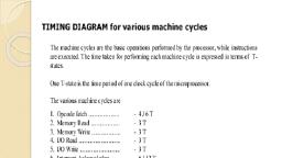
, , Instruction Decoder: It gets the instruction from the instruction register and decodes the, , , , Serial I/O Control: It has two control signals named SID and SOD for serial datatransmission., Timing and Control unit., , , , It has three control signals ALE, RD (Active low) and WR (Active low) and three statussignals, IO/M(Active low), S0 and S1., , , , ALE is used for provide control signal to synchronize the components of microprocessor and timing, for instruction to perform the operation., , , , RD (Active low) and WR (Active low) are used to indicate whether the operation is readingthe data, from memory or writing the data into memory respectively., , , , IO/M(Active low) is used to indicate whether the operation is belongs to the memory or, peripherals., Table 1.3 Machine cycle status and control signals, , 1.5.1The 8085 machine cycles and bus timings: Introduction: A machine cycle is the time required, to complete one operation of accessing the memory, I/O or acknowledge an external signal or request., Usually machine cycle consists of 3 to 6 T-states. In this article let us discuss about their different, types and how they are being classified., Types of machine cycle, There are various types of machine cycles which are classified based onStatus signals (IO/M’, S1, and S0) ,Control Signals (RD’, WR’, INTA)., The different types of machine cycle available in 8085 microprocessor are: Opcode Fetch, Memory ReadMemory writeI/O Read, I/O Write
Page 25 :
INTR AcknowledgeBus Idle, Table 1.4: 8085 machine cycle status and control signals, , Opcode fetch machine cycle: The Opcode fetch cycle, fetches the instructions from memory and, delivers it to the instruction register of the microprocessor. For any instruction cycle, Opcode fetch is, the first machine cycle. We know that each machine cycle may have 3 to 6 T-states. This Opcode fetch, machine cycle consists of 4 T-states., T1 State: During the T1 state, the contents of the program counter are placed on the 16 bit address, bus. The higher order 8 bits are transferred to address bus (A8-A15) and lower order 8 bits are, transferred to multiplexed A/D (AD0-AD7) bus., After the address bits are transferred, the ALE (address latch enable) signal goes high. As soon as, ALE goes high, the memory latches the AD0-AD7 bus. At the middle of the T state the ALE goes, low and the complete 16-bit address is made available for the Opcode fetch machine cycle., T2 State: During the beginning of this state, the RD’ signal goes low to enable memory. It is during, this state, the selected memory location is placed on D0-D7 of the Address/Data multiplexed bus., T3 State: In the previous state the Opcode is placed in D0-D7 of the A/D bus. In this state of the, cycle, the Opcode of the A/D bus is transferred to the instruction register of the microprocessor., Now the RD’ goes high after this action and thus disables the memory from A/D bus., T4 State: In this state the Opcode which was fetched from the memory is decoded., Thus the cycle completes after 4 T-states. This very well explains the Opcode fetch machine cycle. For, better understanding of the concept, a diagram explaining Opcode fetch cycle is shown below., , 26
Page 26 :
Fig 1.21 Memory Read machine cycle, If the instruction is only one byte in length, then one machine cycle is enough to complete the, process (Opcode fetch cycle). When the instruction has more than one byte of information to be, processed, then the microprocessor may require more than one machine cycle to complete the, process. The machine cycle in this case would require reading of address or data from memory or, any other I/O devices. Hence these are known as memory read or I/O read machine cycles. These, machine cycles have 3 T-states., A simple example for memory read machine cycle is MVI D, 24H, For the above example there are 2 machine cycles involved. One is the Opcode fetch cycle and the, second one is the memory read cycle which transfers the operand 24H from the memory to the, microprocessor., T1 state: In this state the contents of the program counter is placed on the higher order address bus, (A8-A15) and lower order address and data multiplexed (AD0-AD7) bus. ALE goes high so that the, memory latches the (AD0-AD7) and then during the middle of the T1 state ALE goes low, so that, complete 16-bit address are available., The microprocessor then identifies the memory read machine cycle from the status signals IO/M’=0,, S1=1, S0=0. This condition indicates the memory read cycle., T2 state: Selected memory location is placed on the (D0-D7) of the A/D multiplexed bus., T3 State: The data which was loaded on the previous state is transferred to the microprocessor. In the, middle of the T3 state RD’ goes high and disables the memory read operation. The data which was, , 27
Page 27 :
obtained from the memory is then decoded., The concept can be understood better with the aid of the diagram shown below., , Fig.1.22 : I/O read machine cycle, This machine cycle is very similar to memory read machine cycle. It is a 2 byte-I/O read instruction., A simple example is IN 22H., The first machine cycle is same as the memory read machine cycle, which is the Opcode fetch cycle., The second machine cycle is the I/O read machine cycle, where the content of port addresses (22H in, this case) is transferred to the microprocessor., The status signal for the I/O read machine cycle is different. The status signal values are IO/M’=1,, S1=1, S0=0., In the next article let us continue with the other 4 types of the machine cycle., , 28
Page 28 :
1.6, MEMORY INTERFACING : Microprocessor need to access memory quite frequently, to readinstructions and data stored in memory; the interface circuit enables that access., , Fig.1.23 Memory Interfacing, The interface process involves designing a circuit that will match the memoryrequirements with the, microprocessor signal.[Memory has certain signalrequirements to read from and write into memory., SimilarlyMicroprocessor initiates the set of signals when it wants to read fromand write into, memory]., , Fig 1.24: Static RAM and EPROM memory, Accessing memory can be summarized into the following three steps:, Select the chip., , 29
Page 29 :
Identify the memory register., Enable the appropriate buffer., And to Translating this to microprocessor domain following steps are required:, The microprocessor places a 16-bit address on the address bus., Part of the address bus will select the chip and the other part will gothrough the address decoder to, select the register., The signals IO/M and RD combined indicate that a memory read operation is in progress. The, MEMR signal can be used to enable theRD line on the memory chip., Address Decoding : The result of ‘address decoding’ is the identification of a register for a given, address. A large part of the address bus is usually connected directly to the address inputs of the, memory chip. This portion is decoded internally within the chip. What concerns us is the other partthat, must be decoded externally to select the chip. This can be done either using logic gates or a decoder., Interfacing circuit :, , Fig 1.25 Interfacing 2732 EPROM with 8085 Microprocessor, The 8085 address lines A11-A0 are connected to the pins A11-A0 of the memory chip.Decoder, decode A15-A12 and output O0 is connected to CE’ which is asserted onlywhen A15-A12 is 0000, (A15 low enables decoder and input 000 asserts the output O0).One control signal MEMR’ is, connected to OE’ to enable output buffer., Example: Interface a 4K EPROM, one 4K RAM and one 8K RAM to a microprocessor withthe, following Memory Map., , 30
Page 30 :
Fig. 1.26 Memory Map, A memory chip select decoder is used to provide chip select signal for eachmemory device (IC). This, will decide the address range that is allotted for each memoryIC. 74LS138 is a 3 to 8 decoder and it can, be used for this purpose. In this example theminimum memory block size is 4K. To access 1K, locations 10 address lines must be used(210 =1K = 1024 locations). So to access 4K locations (4 X, 1K = 22 X 210 = 212) 12address lines (A0 – A11) must be used. Since 8085 has 16 address lines the, decoding can, be indicated as shown below., , Fig 1.27 Variable address lines, , Fig. 1.28: Memory Interface Circuit, , 31
Page 31 :
CHAPTER 2, 2.1 BASIC INTERFACING CONCEPTS, Memory is made up of (registers). Each register consists of one storage location. Each location, consists of an address. The number of storage locations from few hundreds to several mega or giga, locations. The total number of memory storage is calledmemory capacity and measured in Bytes., Each register consists of storage element (FF, capacitor for semiconductor). A storage element is, called cell. The data could be read from or written to memory., 2.1.1 Memory structure and its requirements, Read/write memories consist of an array of registers, in which each register has unique address. The, size of the memory is N x M as shown below where N is the number of registers and M is the word, length, in number of bits., , Fig 2.1 Logic diagram for RAM, If memory is having 12 address lines and 8 data lines, then Number of registers/ memory locations, (capacity) = 2N= 212 = 4096, Word length = M bit = 8 bit, Example 2: If memory has 8192 memory locations, then it has 13 address lines. Table 2.1 shows, how the number of address lines are decided depending on the size of memory., , 32
Page 32 :
Table 2.1 summarizes capacity with address, Memory Capacity, 1k = 1024 memory locations, 2k = 2048 memory locations, 4k = 4096 memory locations, 8k = 8192 memory locations, 16k = 16384 memory locations, 32k = 32768 memory locations, 64k = 65536 memory locations, , Address lines, required, 10, 11, 12, 13, 14, 15, 16, , 2.2 INTERFACING OUTPUT DISPLAYS, The output devices are usually slow. Also the output is usually expected to continue appearing on the, output device for a long period of time. Given that the data will be present on the data lines for a very, short period (microseconds), it has to be latched externally. To do this external latch should be, enabled when the port’s address is present on the address bus, the IO/M signal is high and WR is set, low. The resulting signal would be active when the output device is being accessed by the, microprocessor., 2.3 INTERFACING INPUT DEVICES, The basic concepts are similar to interfacing of output devices. The address lines are decoded to, generate a signal that is active when the particular port is being accessed. An IORD signal is, generated by combining the IO/M and the RD signals from the microprocessor. A tristate buffer is, used to connect the input device to the data bus. The control (enable) for these buffers is connected to, the result of combining the address signal and the signal IORD., 2.4 MEMORY MAPPED I/O, Basic Memory Interfacing with 8085, For interfacing memory devices to µp 8085, following points should be considered:, , , µp 8085 can access 64KB memory since address bus is 16-bit., , , , Generally EPROM (or EPROMs) is used as a program memory and RAM (or RAMs) asdata memory., , , , The capacity of program memory and data memory depends on the application., , , , It is not always necessary to select 1 EPROM and 1 RAM. We can have multiple EPROMs and, multiple RAMs as per the requirement of application., For Example, We have to implement 32 KB of program memory and 4KB EPROMs are available. In this case we can, connect 8 EPROMs in parallel. We can place EPROM/RAM anywhere in full 64 KB address space., But program memory (EPROM) should be located from address 0000 H. It is not always necessary, to locate EPROM and RAM in consecutive memory address. The memory interfacing requires to:, , 33
Page 33 :
Enable the appropriate buffer, , , , Select the chip, Identify the register, , , , , µp system includes memory and I/O devices., It is important to note that µp can communicate (read/write) with only one device at, a time, so address decoding needed., Address Decoding techniques There are two main techniques:, , , , , Absolute decoding/ Full Decoding, Linear decoding / Partial Decoding, Absolute Decoding: All the higher address lines are decoded to select the memory chip, and the, memory chip is selected only for the specified logic level on these high-order address, no other logic, levels can select the chip. The Fig 2.2 shows the memory interface with absolute decoding. This, addressing technique is normally used in large memory systems., , Fig 2.2 Absolute Address Decoding, Linear Decoding- In small systems, h/w for the decoding logic can be eliminated by using, individual high-order address lines to select memory chips. This is referred to as linear decoding., The Fig 2.3 below shows the addressing of RAM with linear decoding technique.This technique is, also called partial decoding. It reduces the cost of the decoding circuit, but it has a drawback of, multiple address (shadow addresses)., , 34
Page 34 :
Fig 2.3 Linear Decoding, Interfacing Examples:, Draw the circuit diagram of an 8085 system, having a 4 KB EPROM and two 8 KB RAM ICs. The, starting address of the EPROM is 0000H and that of RAM is 8000H. The address of the decoder, circuits should be clearly shown., Answer :, EPROM-4 KB (Address lines required is 12 – A0 to A11)RAM-I-8 KB (Address lines required is 13 –, A0 to A12)RAM-II-8 KB (Address lines required is 13 – A0 to A12), Mapping of Addresses to Memory Ics, Table 2.2 Address Mapping, , 35
Page 35 :
Fig 2.4 Address Decoding, 2.5 Flow chart symbols, To develop the programming logic, programmer has to write down various actions which are to be, performed in proper sequence. The flow chart is a graphical tool that allows programmer to, represent various actions which are to be performed. Figure 2.5 shows the graphical symbols used in, flow chart, Fig 2.5 Graphical symbols used in flow chart, 1. Oval: indicates start or stop operation., , 2. Arrow: indicates flow with direction, 3. Parallelogram: indicates input/output operation., 4. Rectangle: indicates process operation, 5. Diamond: indicates decision making operation, , 38
Page 36 :
6. ouble sided rectangle: indicates execution of3s7ubroutine, 7. Circle with alphabet: indicates continuation., 2.6 DATA TRANSFER INSTRUCTIONS, Opcode, source to destination, MOV Rd, Rs M, Rs Rd, M, , Move immediate 8-bit, MVI Rd, data M, data, , Load accumulator, LDA 16-bit address, , Load accumulator indirect, LDAX B/D Reg.pair, , Store accumulator direct, STA 16-bit address, , Store accumulator indirect, , Operand, , DescriptionCopy from, , This instruction copies the contents of the source, register into the destination register; the contents of, the source register are not altered. If one of the, operands is a memory location, its location is specified, by the contents of the HL registers., Example: MOV B, C or MOV B, M, The 8-bit data is stored in the destination register or, memory. If the operand is a memory location, its, location is specified by the contents of the HL, registers., Example: MVI B, 57 or MVI M, 57, , The contents of a memory location, specified by a16bit address in the operand, are copied to the, accumulator. The contents of the source are not altered., Example: LDA 2034 or LDA XYZ, , The contents of the designated register pair point to a, memory location. This instruction copies the contents, of that memory location into the accumulator. The, contents of either the register pair or the memory, location are not altered., Example: LDAX B, The contents of the accumulator are copied into the, memory location specified by the operand. This is, a 3-byte instruction, the second byte specifies the loworder address and the third byte specifies the highorder address., Example: STA 4350 or STA XYZ, , Reg. pair The contents of the accumulator are copied into the memory location specified by the contents of, the operand (register pair). The contents of the accumulator are not altered., Example: STAX B, , 39
Page 37 :
Load register pair immediate, LXI Reg. pair, 16-bit data The instruction loads 16-bit data in the register pair designated in the, operand.Example: LXI H, 2034, Load H and L registers direct, The instruction copies the contents of the memory location pointed out by the 16-bit address into, register L and copies the contents of the next memory location into, register H. The contents of source memory locations arenot altered., Example: LHLD 2040, Store H and L registers direct, The contents of register L are stored into the memory location specified by the 16-bit address in, the operand and the contents of H register are stored into the next memory location by incrementing, the operand. The contents of registers HL are not altered. This is a 3-byte instruction, the second byte, specifies the low-order address and the third byte specifies the high-order address., Example: SHLD 2470, Exchange H and L with D and E XCHG none, The contents of register H are exchanged with the contentsof register D, and the contents of register L, are exchanged with the contents of register E., Example: XCHG, 2.7 ARITHMETIC INSTRUCTIONS, Opcode, ADD, , Operand, DescriptionAdd register or memory to accumulator, R, The contents of the operand (register or memory) arM, the contents of the accumulator and the result is stored in the accumulator. If the, operand is a memory location, its location is specified by the contents of the HLregisters. All flags are, modified to reflect the result of the addition., Example: ADD B or ADD M, Add register to accumulator with carry, ADC, R, The contents of the operand (register or memory), and the, M, Carry flag are added to the contents of the accumulator and the result is, stored in the accumulator. If the operand is a memory location, its, location is specified by the contents of the HL registers. All flags are, modified to reflect the result of theaddition., Example: ADC B or ADC M, , Add immediate to accumulator, , 40
Page 38 :
ADI 8-bit data, The 8-bit data (operand) is added to the contents of the, accumulator and the result is stored in the accumulator. All flagsare modified to reflect the result of the, addition., Example: ADI 45, Add immediate to accumulator with carry, The 8-bit data (operand) and the Carry flag are added to thecontents of the accumulator and the result, is stored in the accumulator. All flags are modified to reflect the result of the addition., Example: ACI 45, Add register pair to H and L registers, The 16-bit contents of the specified register pair are added to the contents of the HL register and the, sum is stored in the HL register. The contents of the source register pair arenot altered. If the result is, larger than 16 bits, the CY flag isset. No other flags are affected., Example: DAD H, The contents of the operand (register or memory ) are subtracted from the, SUB R contents of the accumulator, and the result is stored in the accumulator. If, M the operand is a memory location, its location is specified by the contents, of the HL registers. All flags are modified to reflect the result of the, subtraction., Example: SUB B or SUB M, Subtract source and borrow from accumulator, SBB, R The contents of the operand (register or memory ) and the, Borrow flag are subtracted from the contents of the accumulator and the result is placed in the, accumulator. If the operand is a memory location, its location is specified by the contents of the HL, registers. All flags are modified to reflect the result in accumulator., Example: SBB B or SBB M, Subtract immediate from accumulator, The 8-bit data (operand) is subtracted from the contents of the accumulator and the result is stored in, the accumulator. All flags are modified to reflect the result of the subtraction., Example: SUI 45, Subtract immediate from accumulator with borrow, The 8-bit data (operand) and the Borrow flag are subtracted from the contents of the accumulator, and the result is stored in the accumulator. All flags are modified to reflect the result of the, subtracion., Example: SBI 45, , 41
Page 39 :
Increment register or memory by 1INR R, M, Increment register pair by 1, The contents of the designated register or memory) are incremented by 1 and the result is stored in, the same place. If the operand is a memory location, its location is specified by the contents of the HL, registers., Example: INR B or INR M, The contents of the designated register pair are incremented by1 and the result is stored in the same, place., Example: INX H, Decrement register or memory by 1, DCR R, M, , The contents of the designated register or memory are, decremented by 1 and the result is stored in the same place. If the, operand is a memory location, its location is specified by the, contents of the HL registers., Example: DCR B or DCR M, , Decrement register pair by 1, , 42
Page 40 :
The contents of the designated register pair are decremented by 1 and the result is stored in the, same place. Example: DCX H, Decimal adjust accumulator, The contents of the accumulator are changed from a binary value to two 4-bit binary coded decimal, (BCD) digits. This is the only instruction that uses the auxiliary flag to perform the binary to BCD, conversion, and the conversion procedure is described below. S, Z, AC, P, CY flags are altered to, reflect the results of the operation., If the value of the low-order 4-bits in the accumulator is greater than 9 or if AC flag is set, the, instruction adds 6 to thelow-order four bits., If the value of the high-order 4-bits in the accumulator is greater than 9 or if the Carry flag is set, the, instruction adds 6to the high-order four bits., Example: DAA, 2.8 LOGICALINSTRUCTIONS, Opcode, , Operand, , DescriptionCompare register or memory with, , accumulator, CMP, R, The contents of the operand (register or, memory) are, compared with the contents of the accumulator. Bothcontents are preserved . The result of the, comparison is shown by setting the flags of the PSW as follows:if (A) < (reg/mem): carry flag is set,, s=1, if (A) = (reg/mem): zero flag is set, s=0, if (A) > (reg/mem): carry and zero flags are reset, s=0 Example: CMP B or CMP M, Compare immediate with accumulator, The second byte (8- bit data) is compared with the contents of the accumulator. The values being, compared remain unchanged. The result of the comparison is shown by setting the flags of the PSW, as follows:, if (A) < data: carry flag is set, s=1if (A) = data: zero flag is set, s=0, if (A) > data: carry and zero flags are reset, s=0 Example: CPI 89, Logical AND register or memory with accumulator, ANA, , RM, , The contents of the accumulator are logically ANDed with the contents, of the operand (register or memory), and the result is placed in the, accumulator. If the operand is a memory location, its address is, specified by the contents of HL registers. S, Z, P are modified to reflect, the result of the operation. CY is reset. AC is set., Example: ANA B or ANA M, , Logical AND immediate with accumulator, The contents of the accumulator are logically, ANI, 8-bit data, ANDed with, the 8-bit data (operand) and the result is placed in the accumulator. S, Z, P are modified to reflect the, , are affected4.3Example: CMA
Page 41 :
result of theoperation. CY is reset. AC is set., Example: ANI 86, Exclusive OR register or memory with accumulator, XRA, RM, The contents of the accumulator are Exclusive ORed with the contents, of the operand (register or memory), and the result is placed in the, accumulator. If the operand is a memory location, its address is, specified by the contents of HL registers. S, Z, P are modified to, reflect the result of the operation. CY and AC are reset., Example: XRA B or XRA M, Logical OR register or memory with accumulator, , are affected4.3Example: CMA
Page 42 :
ORA, , 45, , RM
Page 43 :
The contents of the accumulator are logically ORed with the contents of the operand, (register/memory), and the Result is placed in the accumulator. If the operand is a memory location,, its address is specified by the contents of HL registers. S, Z, P are modified to reflect the result of the, operation. CY and AC are reset., Example: ORA B or ORA M, Exclusive OR immediate with accumulator, The contents of the accumulator are Exclusive ORed with the 8-bit data (operand) and the result is, placed in the accumulator. S, Z, P are modified to reflect the result of the operation. CY and AC are, reset., Example: XRI 86, Logical OR immediate with accumulator, The contents of the accumulator are logically ORed with the 8-bit data (operand) and the result is, placed in the accumulator. S, Z, P are modified to reflect the result of the operation. CY and AC are, reset., Example: ORI 86, Complement accumulator, CMA none, No flags, , The contents of the accumulator are complemented., , Complement carry, CMC none, affected., , The Carry flag is complemented. No other flags are, Example: CMC, , Set Carry, STC none, , The Carry flag is set to 1. No other flags are affected., Example: STC, , 2.9 BRANCHING INSTRUCTIONS, Opcode, Operand, DescriptionJump unconditionally, JMP, 16-bit address, The program sequence is transferred to the memory, location, specified by the 16-bit address given in the operand.Example: JMP 2034 or JMP XYZ, Jump conditionally, Operand: 16-bit address, The program sequence is transferred to the memory location specified by the 16- bit address given in, the operand based onthe specified flag of the PSW as described below., Example: JZ 2034 or JZ XYZ, Opcode, JC, JNC, JP, JM, JZ, , Description, Jump on Carry, Jump on no Carry, Jump on positive, Jump on minus, Jump on zero, , Flag Status, CY = 1, CY = 0, S=0, S=1, Z=1, , 46
Page 44 :
JNZ, JPE, JPO, , Jump on no zero, Jump on parity even, Jump on parity odd, , Z=0, P=1, P=0, , Unconditional subroutine call, CALL, 16-bit address, The program sequence is transferred to the memory, location, specified by the 16-bit address given in the operand. Before the transfer, the address of the next, instruction after CALL (the contents of the program counter) is pushed onto the stack.Example:, CALL 2034 or CALL XYZ, Call conditionally Operand: 16-bit address, The program sequence is transferred to the memory location specified by the 16-bit address given in, the operand based on the specified flag of the PSW as described below. Before the transfer, the, address of the next instruction after the call (the contents of the program counter) is pushed onto the, stack., Example: CZ 2034 or CZ XYZ, , Opcode Description, Call on Carry, CNC Call on no Carry, CP, Call on positive, CM, Call on minus, CZ, Call on zero, CNZ Call on no zero, CPE Call on parity even, CPO Call on parity odd, , Flag Status, CY = 1, CY = 0, S=0, S=1, Z=1, Z=0, P=1, P=0, , CC, , Return from subroutine unconditionally, The program sequence is transferred from the subroutine to the calling program. The two bytes, from the top of the stack are copied into the program counter, and program execution begins at the, new address., Example: RET, Return from subroutine conditionally, Operand: none, The program sequence is transferred from the subroutine to the calling program based on the, specified flag of the PSW as described below. The two bytes from the top of the stack are copied into, the program counter, and program execution begins at the new address., Example: RZ, , 47
Page 45 :
Opcode, RC, RNC, RP, RM, RZ, RNZ, RPE, RPO, , Description, Return on Carry, Return on no Carry, Return on positive, Return on minus, Return on zero, Return on no zero, Return on parity even, Return on parity odd, , Flag Status, CY = 1, CY = 0, S=0, S=1, Z=1, Z=0, P=1, P=0, , Load program counter with HL contents, The contents of registers H and L are copied into the program counter. The contents of H are placed, as the high-order byte and the contents of L as the low-order byte., Example: PCHL, Restart, The RST instruction is equivalent to a 1-byte call instruction to one of eight memory locations, depending upon the number. The instructions are generally used in conjunction with interrupts and, inserted using external hardware. However these can be used as software instructions in a, program to transfer program execution to one of the eight locations. Theaddresses are:, Instruction, RST 0, RST 1, RST 2, RST 3, RST 4, RST 5, RST 6, RST 7, , Restart Address, 0000H, 0008H, 0010H, 0018H, 0020H, 0028H, 0030H, 0038H, , The 8085 has four additional interrupts and these interrupts generate RST instructions internally and, thus do not require any external hardware. These instructions and their Restart addresses are:, Interrupt, , Restart Address, , TRAP, RST 5.5, RST 6.5, RST 7.5, , 0024H, 002CH, 0034H, 003CH, , 2.10 WRITING ASSEMBLY LANGUAGE PROGRAMMS, 1., Store the data byte 32H into memory location 4000H. MVI A, 52H : Store 32H inthe, accumulator, STA 4000H :, HLT :, , Copy accumulator contents at address 4000H, Terminate program execution, , 48
Page 46 :
Program 2:, LXI H :, MVI M :, register pair, HLT :, 2., , Load HL with 4000H, Store 32H in memory location pointed by HL, Terminate program execution, Exchange the contents of memory locations 2000H and 4000H.Program 1:, , LDA 2000H, : Get the contents of memory location 2000H into accumulatorMOV, B, A, : Save the contents into B register, LDA 4000H, : Get the contents of memory location 4000Hinto accumulatorSTA, Get the contents of mem4o6ry location 4000H into A register, LDAX D 2000H, : Store the contents of accumulator at address 2000H, MOV A, B, : Get the saved contents back into A register, STA 4000H : Store the contents of accumulator at address 4000HProgram 2:, LXI H 2000H, LXI D 4000H, MOV B, M, MOV M, A, A, B, STAX D, , : Initialize HL register pair as a pointer to memory location 2000H., : Initialize DE register pair as a pointer to memory location 4000H., : Get the contents of memory location 2000H into B register., : Store the contents of A register into memory location 2000H.MOV, : Copy the contents of B register into accumulator., : Store the contents of A register into memory location 4000H. HLT, : Terminate program execution., , 3., Find the 2's complement of the number stored at memory location 4200H and store the, complemented number at memory location 4300H., Source program:, LDA 4200H, CMA, ADI, 01 H, STA 4300H, HLT, , : Get the number, : Complement the number, : Add one in the number, : Store the result, : Terminate program executionFlow chart:, Fig 2.6 Flow Chart, , 49
Page 50 :
Fig 2.10 Flow Chart, Source program:, LDA 4200H : Get the packed BCD number ANI FOH : Mask lower nibble, RRCRRCRRC, RRC : Adjust higher BCD digit as a lower digitSTA 4301H : Store the partial result, LDA 4200H : .Get the original BCD number ANI OFH : Mask higher nibble, STA 4201H : Store the result, HLT : Terminate program execution, ADDRESSING MODES, Every instruction of a program has to operate on a data. The method of specifying the data to be, operated by the instruction is called Addressing., The 8085 has the following 5 different types of addressing., , 53
Page 51 :
1. Immediate Addressing, 2. Direct Addressing,, 3. Register Addressing, 4. Register Indirect Addressing, 5. Implied Addressing, Immediate Addressing, In immediate addressing mode, the data is specified in the instruction itself. The data will be apart of, the program instruction. All instructions that have ‘I’ in their mnemonics are of Immediate, addressing type., Eg.MVI B, 3EH- Move the data 3EH given in the instruction to B register., Direct Addressing, In direct addressing mode, the address of the data is specified in the instruction. The data will be in, memory. In this addressing mode, the program instructions and data can be stored in, differentmemory blocks. This type of addressing can be identified by 16bit address present in theinstruction., Eg.LDA 1050H- Load the data available in memory location 1050H in accumulator., Register Addressing, In register addressing mode, the instruction specifies the name of the register in which the data is, available. This type of addressing can be identified by register names (such as ‘A’, ‘B’ .................... ) in the, instruction., Eg. MOV A, B -Move the content of B register to A register., Register Indirect Addressing, In register indirect addressing mode, the instruction specifies the name of the register in which the, address of the data is available. Here the data will be in memory and the address will be in the, register pair. This type of addressing can be identified by letter ‘M’ present in the instruction., Eg. MOV A, M - The memory data addressed by HL pair is moved to A register., Implied Addressing, In implied addressing mode, the instruction itself specifies the type of operation and location of data, to be operated. This type of instruction does not have any address, register name, immediate data, specified along with it. Eg. CMA - Complement the content of accumulator, 2.11 PROGRAMMING TECHNIQUES, Looping-In this technique, the program is instructed to execute certain set of instructions repeatedly, toexecute a particular task number of times., Counting-This technique allows programmer to count how many times the instruction/set of, instructionsare executed., Indexing-This technique allows programmer to point or refer the data stored in sequential, memorylocation one by one., , 54
Page 52 :
CHAPTER 3, 3.1 ADDITIONAL DATA TRANSFER AND 16 BIT ARITHMETIC INSTRUCTION, The data transfer operations are:, 1.MVI rd , byte :- This instruction moves the immediate data givenafter the instruction into register rd., 2.MOV rd , rs :- This instruction moves data from register rs toregister rd., 3. LXI rp, 16-bit:- This instruction moves 16-bit data or address toregister pair., 4., XCHG: The contents of register H are exchanged with the contents of register D, and the, contents ofregister L are exchanged with thecontents of register E., 3.2 ARITHMETIC OPERATIONS RELATED TO MEMORY, Examples:, 1., Calculate the sum of series of numbers. The length of series is in memory location, 2200H and seriesitself begins from 2201H., (a) Assume the sum to be 8 bit number, so ignore carry. Store the sum at 2300H., (b), Assume the sum to be 16 bit number. Store the sum at memory locations 2300H &, 2301H.(a), LDA 2200HMOV C,A SUB A, LXI H, 2201H, BACK: ADD M INX H DCR C, JNZ BACKSTA 2300HHLT, (b), LDA 2200H MOV C,A LXI H,2201HSUB A, MOV B, A, Y: ADD M JNC XINR B INX HDCR CJNZ Y, STA 2300HMOV A, B STA 2301HHLT, 2., Multiply two 8-bit numbers stored in memory location 2200H & 2201H. Store the, result in memorylocation 2300H & 2301H., , LDA 2200H, , 53
Page 54 :
Rotate accumulator left through carry, , 57
Page 56 :
Each binary bit of the accumulator is rotated right by one position. Bit D0 is placed in the position of, D7 as well as in the Carry flag. CY is modified according to bit D0. S, Z, P,AC are not affected., Example: RRC, Each binary bit of the accumulator is rotated left by one position through the Carry flag. Bit D7 is, placed in the Carryflag, and the Carry flag is placed in the least significant position D0. CY is, modified according to bit D7. S, Z, P, ACare not affected. Example:RAL, Rotate accumulator right through carry, Each binary bit of the accumulator is rotated right by one position through the Carry flag. Bit D0 is, placed in the Carryflag, and the Carry flag is placed in the most significant position D7. CY is, modified according to bit D0. S, Z, P, ACare not affected. Example:RAR, Compare register or memory with accumulator, CMP, R, The contents of the operand (register or memory) are, compared with the contents of the accumulator. Bothcontents are preserved . The result of the, comparison is shown by setting the flags of the PSW as follows:, if (A) < (reg/mem): carry flag is set, s=1 if (A), = (reg/mem): zero flag is set, s=0, if (A) > (reg/mem): carry and zero flags are reset, s=0Example: CMP B or CMP M, Compare immediate with accumulator, The second byte (8- bit data) is compared with the contents of the accumulator. The values being, compared remain unchanged. The result of the comparison is shown by setting the flags of the PSW, asfollows:, if (A) < data: carry flag is set, s=1 if (A), = data: zero flag is set, s=0, if (A) > data: carry and zero flags are reset, s=0Example: CPI 89, 3.4 COUNTER AND TIME DELAYS, A loop counter is set up by loading a register with certain value. Then using DCR and INR the contents, of register are modified. A loop is set up with a conditional jump that looks back or not depending on, whether the count has reached the termination count. The operation of a counter can be described using, flow chart as shown in Figure 3.4, , 69
Page 57 :
Fig 3.3Flow Chart, Implementing loop using DCR instruction:MVI C, 15H, LOOP:DCR C, JNZ LOOP, Using a register pair as a loop counter:, Using a single register, one can repeat a loop for maximum 255 times., LXI B, 100HLOOP: DCX B, MOV A, CORA B JNZ LOOP, Delay Routine, Delay routines are subroutines used for maintaining the timings of various operations inmicroprocessor.In, control applications, certain equipment needs to be ON/OFF after a specified time delay. In some, applications, a certain operation has to be repeated after a specified time interval. In such cases,, simple time delay routines can be used to maintain the timings of the operations., DELAY ROUTINE PROCESS, A delay routine is generally written as a subroutine (It need not be a subroutine always. It can, beeven a part of main program). In delay routine a count (number) is loaded in a register of, microprocessor. Then it is decremented by one and the zero flag is checked to verify whether, thecontent of register is zero or not. This process is continued until the content of register is, zero.When it is zero, the time delay is over and the control is transferred to main program to carry out, the desired operation., The delay time is given by the total time taken to execute the delay routine. It can be computed by, multiplying the total number of T-states required to execute subroutine and the time for one T-state of, the processor. The total number of T-states can be computed from the knowledge of T-states required, for each instruction. The time for one T-state of the processor is given by the inverse of the internal, clock frequency of the processor., For example, if the 8085 microprocessor has 5 MHz quartz crystal then, the internal clock frequency =, 5 /2 = 2.5 MHz, Time for one T-state= 1 / 2.5 x 106= 0.4µsec, • For small time delays (< 0.5 msec) an 8- bit register can be used., • For large time delays (< 0.5 Sec) l6-bit register should be used., •, For very large time delays (> 0.5 sec), a delay routine can be repeatedly, called in themain program., The disadvantage in delay routines is that the processor time is wasted. An alternate solution is to, usededicated timer like 8253/8254 to produce time delays or to maintain timings of various, operations., EXAMPLE DELAY ROUTINE, 1., Write a delay routine to produce a time delay of 0.5 msec in 8085 processor-based, system whose clocksource is 6 MHz quartz crystal., Solution, , 70
Page 58 :
The delay required is 0.5 msec, hence an 8-bit register of8085 can be used to store a Count value and, thendecrement to zero. The delay routine is written as a subroutine as shown below., Delay routine, Loop: DCR D, JNZ Loop, RET, , ; Decrement the count., ; If count is zero go to, ; Return to main program., , The following table shows the T-state required for execution of the instructions in the subroutine., Table 3.1 Calculation to find the count value, Instruction, T-State requiredfor, Number of times, execution of, theinstruction is, aninstruction, executed, CALL addr16, 18, 1, MVI D, N, 7, 1, DCR D, 4, N times, JNZ LOOP, 10, (N-1) times, 7, 1, RET, 10, 1, TOTAL T-STATES FOR DELAY SUBROUTINE, , Total T-States, , 18 x 1 = 18, 7x1=7, 4 x N = 4N, 10 x (N-1) = 10N – 10, 7x1=7, 10 x 1 = 10, 14N + 32, , Calculation to find the count value, N:, External clock frequency = 6 Mhz, Internal clock frequency = External Frequency / 2= 6 / 2= 3 Mhz, Time period for 1 T-State= 1 / Internal clock frequency= 1 / 3x106= 0.333µS, No. of T-states requiredfor delay of 0.5mS = Required time delay / Time for one T-state, = 0.5mS / 0.333µS= 1500.10≈ 1500 = 150010, From above table, we know that;14N + 32 = 1500, N = (1500 – 32) / 14 = 104.85710≈ 10510= 69H, Therefore by replacing the count value, N by 69H in the above program , a delay of 0.5mSec can, beproduced, 2., Write an ALP for 8085 to count from AAHto 00H, with a time delay of 2ms for each, count. Assumethe external frequency given to the processor is 2MHz., Internal Frequency in 8085 = External frequency / 2ie.,= 2Mhz / 2= 1Mhz1, T-State= 1 / f (internal frequency)= 1µS, Main program for counting from AA to 00, MVI C, AAH, Loop:CALL Delay, DCR C, JNZ LoopHLT, Delay program for delay of 2ms, , 71
Page 60 :
Program:, MVI A, 64H, X: OUT PORT1, Y:MVI B, 10H, Z:LXI D, X, DCX D, NOP, NOP, MOV A, D, ORA E, JNZ Z, DCR B, JZ Y, DCR A, CPI 00H, JNZ X, , 7, 10, 7, 10, 6, 4, 4, 4, 4, 10/7, 4, 10/7, 4, 7, 10/7, , Delay in loop1=32T X count x 330x10-9, 100ms =32T X count x 330x10-9, Count=9470, 3.6 STACK, SUBROUTINE, It is a part of memory, reserved in RAM, used to temporarily store information during execution of, program. Starting address of stack is loaded in stack pointer (a 16 bit register). The address pointed by, SP is known as top of stack, which is always an empty memory location. Stack can be defined, loss. The figure shows the stack initialization. Stack is LIFO type of memory. When information is, stored onto stack, the SP decrements the pointer to lower empty address. When information is read, from stack, the SP register increments to higher empty address., , Fig 3.4 stack initialization, STACK INSTRUCTIONS, , 73
Page 61 :
Copy H and L registers to the stack pointer, The instruction loads the contents of the H and L registers into the stack pointer register, the, contents of the H register provide the high-order address and the contents of the L register provide, the low-order address. The contents of the H and L registers are not altered., Example: SPHL, Exchange H and L with top of stack, The contents of the L register are exchanged with the stack location pointed out by the contents of, the stack pointer, register. The contents of the H register are exchanged with the next stack location (SP+1); however,, the contents of thestack pointer register are not altered., Example: XTHL, Push register pair onto stack, The contents of the register pair designated in the operand are copied onto the stack in the following, sequence. The stack, pointer register is decremented and the contents of the high- order register (B, D, H, A) are copied, into that location. The stack pointer register is decremented again and the contents of the low- order, register (C, E, L, flags) are copied to that location., Example: PUSH B or PUSH A, Pop off stack to register pair, The contents of the memory location pointed out by the stack pointer register are copied to the, low-order register (C, E, L, status flags) of the operand. The stack pointer is incremented by 1 and, the contents of that memory location are copied to the high-order register (B, D, H, A) of the, operand. The stack pointer register is again incremented by 1., Example: POP H or POP A, Subroutine, A subroutine is a group of instructions that will be used repeatedly in different locations of the, program. Rather thseveral times, they can be grouped into a subroutine that is called from different, locations. The 8085 has two instr, 1. The CALL instruction is used to redirect program execution to the subroutine, 2. The RET instruction is used to return the execution of the calling routine., 3.7 RESTART, CONDITIONAL CALL AND RETURN INSTRUCTIONS, Call conditionally, Operand: 16-bit address, The program sequence is transferred to the memory location specified by the 16-bit address given in, the operand based on the specified flag of the PSW as described below. Before the transfer, the, address of the next instruction after the call (the contents of the program counter) is pushed onto the, stack., Example: CZ 2034 or CZ XYZ, , 74
Page 62 :
Opcode, CC, CNC, CP, CM, CZ, CNZ, CPE, CPO, , Description, Call on Carry, Call on no Carry, Call on positive, Call on minus, Call on zero, Call on no zero, Call on parity even, Call on parity odd, , Flag Status, CY = 1, CY = 0, S=0, S=1, Z=1, Z=0, P=1, P=0, , Return from subroutineunconditionally, RE none, The program sequenc is transferred from the subroutine to thecalling program. The two bytes from, the top of the stack are copied into the program counter, and program execution begins at the new, address., Example: RET, Return from subroutine conditionally, Operand: none, The program sequence is transferred from the subroutine to the calling program based on the, specified flag of the PSW as described below. The two bytes from the top of the stack are copied into, the program counter, and program execution begins at the new address., Opcode, RC, RNC, RP, RM, RZ, RNZ, RPE, RPO, 3.8, Opcode, , Description, Return on Carry, Return on no Carry, Return on positive, Return on minus, Return on zero, Return on no zero, Return on parity even, Return on parity odd, , Flag Status, CY = 1, CY = 0, S=0, S=1, Z=1, Z=0, P=1, P=0, , ADVANCE SUBROUTINE CONCEPTSControl Instructions, Operand, , No operation, none, , No operation is performed. The instruction is fetched anddecoded. However no operation is, executed., Example: NOP, Halt and enter wait state, none The CPU finishes executing the current instruction and halts anyfurther execution. An interrupt, or reset is necessary to exit from the halt state. Example: HLT, Disable interrupts, none The interrupt enable flip-flop is reset and all the interrupts except the TRAP are disabled. No, flags are affected. Example: DI, , 75
Page 63 :
Enable interrupts, none The interrupt enable flip-flop is set and all interrupts are enabled. No flags are affected. After, a system reset or the acknowledgement of an interrupt, the interrupt enable flip-flop is reset, thus, disabling the interrupts. This instruction is necessary to reenable the interrupts (except TRAP)., Example: EI, Read interrupt mask, This is a multipurpose instruction used to read the status ofinterrupts 7.5, 6.5, 5.5 and read serial, data input bit. Theinstruction loads eight bits in the accumulator with thefollowing interpretations., Example: RIM, , 76
Page 64 :
Fig 3.5 RIM Structure, , Set interrupt mask, none, This is a multipurpose instruction and used to implement the8085 interrupts, 7.5, 6.5, 5.5, and serial data output.The instructioninterprets the accumulator contents as follows., Example, , Fig 3.6 SIM Structure, Input/Output Instructions, Output data from accumulator to a port with 8-bit address, OUT 8-bit port address The contents of the accumulator are copied into the, I/O port specified by the operand. Example: OUT 87, Input data to accumulator from a port with 8-bit address, , 77
Page 65 :
The contents of the input port designated in the operand are read and loaded into the accumulator., Example: IN 82, , 3.9 THE 8085 INTERRUPTS, Interrupt is a signal send by an external device to the processor, to the processor to perform a, particular task or work. Mainly in the microprocessor based system the interrupts are used for data, transfer between the peripheral and the microprocessor., When a peripheral is ready for data transfer, it interrupts the processor by sending an appropriate, signal to the interrupt pin of the processor. If the processor accepts the interrupt then the processor, suspends its current activity and executes an interrupt service subroutine to complete the data transfer, between the peripheral and processor. After executing the interrupt service routine the processor, resumes its current activity. This type of data transfer scheme is called interrupt driven data transfer, scheme., Types of Interrupts, The interrupts are classified into software interrupts and hardware interrupts., •, The software interrupts are program instructions. These instructions are inserted at, desired locations in a program. While running a program, lf a software interrupt instruction is, encountered, then the processor executes an interrupt service routine (ISR)., •, The hardware interrupts are initiated by an external device by placing an appropriate, signal at the interrupt pin of the processor. If the interrupt is accepted, then the processor executes an, interrupt service routine (ISR)., Software Interrupts Of 8085, The software interrupts are program instructions. When the instruction is executed, the, processor executes an interrupt service routine stored in the vector address of the software interruptinstru, ction. The software interrupts of 8085 are RST 0, RST 1, RST 2, RST 3, RST 4, RST 5, RST6 and, RST, 7., Table 3.2 Vector address for software interrupts, Interrupt, RST0, RST1, RST2, RST3, RST4, RST5, RST6, RST7, , Vector address, 0000H, 0008H, 0010H, 0018H, 0020H, 0028H, 0030H, 0038H, , The software interrupt instructions are included at the appropriate (or required) place in the, , 78
Page 66 :
main program. When the processor encounters the software instruction, it pushes the content of, PC(Program Counter) to stack. Then loads the Vector address in PC and starts executing the, Interrupt Service Routine (ISR) stored in this vector address. At the end of ISR, a return instruction –, RET will be placed. When the RET instruction is executed, the processor POP the content of stack to, PC. Hence theprocessor control returns to the main program after servicing the interrupt., Execution of ISR is referred to as servicing of interrupt. All software interrupts of 8085 are vectored, interrupts. The software interrupts cannot be masked and they cannot be disabled. The software, interrupts are RST0, RST1, … RST7 (8 Nos)., Hardware Interrupts Of 8085, An external device, initiates the hardware interrupts of 8085 by placing an appropriate signal at the, interrupt pin of the processor. The processor keeps on checking the interrupt pins at the second Tstate of last machine cycle of every instruction. If the processor finds a valid interrupt signal and if, the interrupt is unmasked and enabled, then the processor accepts the interrupt. The acceptance of, the interrupt is acknowledged by sending an INTA signal to the interrupted device. The processor, saves the content of PC (program Counter) in stack and then loads the vector address of the interrupt in, PC. (If the interrupt is non-vectored, then the interrupting device has to supply the address of ISR, when it receives INTA signal). It starts executing ISR in this address. At the end of ISR, a return, instruction, RET will be placed. When the processor executes the RET instruction, it POP the content, of top of stack to PC. Thusthe processor control returns to main program after servicing interrupt., The hardware interrupts of 8085 are TRAP, RST 7.5, RST 6.5, RST 5.5 and INTR, Further the interrupts may be classified into VECTORED and NON-VECTORED INTERRUPTS., 1., VECTORED INTERRUPT- In vectored interrupts, the processor automatically, branches to thespecific address in response to an interrupt., 2., NON-VECTORED INTERRUPT- But in non-vectored interrupts the interrupted, device should givethe address of the interrupt service routine (ISR)., 3.9.1 8085 vector interrupts, In vectored interrupts, the manufacturer fixes the address of the ISR to which the program control is, tobe transferred. The vector addresses of hardware interrupts are given in table as shown below:, Hardware interrupts:, Table 3.3 Vector address for interrupts, Interrupt, RST 7.5, RST 6.5, RST 5.5, TRAP, , Vector address, 003CH, 0034H, 002CH, 0024H, , The TRAP, RST 7.5, RST 6.5 and RST 5.5 are vectored interrupts. The INTR is a non-vectored, interrupt. Hence when a device interrupts through INTR, it has to supply the address of ISR after, receiving interrupt acknowledge signal., The TRAP interrupt is edge and level sensitive. Hence, to initiate TRAP, the interrupt signal has to, makea low to high transition and then it has to remain high until the interrupt is recognized., , 79
Page 67 :
The RST 7.5 interrupt is edge sensitive (positive edge). To initiate the RST 7.5, the interrupt signal, hasto make a low to high transition an it need not remain high until it is recognized., The RST 6.5, RST 5.5 and INTR are level sensitive interrupts. Hence for these interrupts the, interrupting signal should remain high, until it is recognized., MASKABLE & NON-MASKABLE INETRRUPTS:, The hardware vectored interrupts are classified into maskable and non-maskable interrupts., •TRAP is non-maskable interrupt, •, RST 7.5, RST 6.5 and RST 5.5 are maskable interrupt. Masking is preventing the, interrupt from disturbing the main program. When an interrup7t1is masked the processor will not, accept the interrupt signal. The interrupts can be masked by moving an appropriate data (or code) to, accumulator and then executing SIM instruction. (SIM - Set InterruptMask). The status of maskable, interrupts can be read into accumulator by executing RIM instruction (RIM - Read Interrupt, Mask).All the hardware interrupts, except TRAP are disabled, when the processor is resetted. They, can also be disabled by executing Dl instruction. (Dl-Disable Interrupt)., •, When an interrupt is disabled, it will not be accepted by the processor. (i.e., INTR, RST, 5.5, RST 6.5and RST 7.5 are disabled by DI instruction and upon hardware reset)., •, To enable (to allow) the disabled interrupt, the processor has to execute El, instruction (El-EnableInterrupt)., Compare CALL and JMP instructions., CALL Instruction:Execution of a CALL instruction will transfer the program control from existing, program toanother program. i.e., Sub program specified by the 16-bit address in CALL instruction, will be executed. The called program should have RET – return instruction as its last instruction.Time, taken for its execution is 9 / 18T, Main, addr16:, , CALL addr16, , RET, JMP Instruction, Execution of a JMP instruction will transfer the program control from one location toanotherlocation, within the same program. Time taken for its execution is 7 / 10T, Main, , 80
Page 70 :
Flow chart:, , Fig. 4.2 Flow chart fo7r7 binary to BCD conversion
Page 72 :
Flow chart:, Fig. 4.2 Flow chart fo7r7 binary to BCD conversion
Page 79 :
4.8 ADVANCED INSTRUCTIONS, , 1., LHLD Address(16 bit)- This instruction is used to load the contents of memory, location given within the instruction into L register and the contents of memory location next to it, willbe stored in H register., Example: LHLD 5000H- It will load the contents of memory location 5000H into L register andthe, contents of memory location 5001H will be stored in H register., 2., SHLD Address(16 bit)- This instruction will store the contents of L register into the, memory address as specified within the instruction and store the contents of H register into memory, location next to it., Example: SHLD 5000H- This instruction will store the contents of L register into the memory, address 5000 and store the contents of H register into memory location 5001., 3., XCHG- This instruction is used to exchange the contents of HL register pair with the, contents of DE register pair., 4., XTHL- This instruction is used to exchange the contents of HL register pair with the, contents of top of stack., 5. SPHL- This instruction is used to copy the contents of HL register pair into top of stack., 6., counter., , PCHL- This instruction is used to copy the contents of HL register pair into program, , 7., ADC R- This instruction is used to add the contents of accumulator with the contents, of specified register and carry and store the result in accumulator., 8., ADC M- This instruction is used to add the contents of accumulator with the contents, of memory location as pointed by HL register pair and carry and store the result in accumulator., 9., ACI Data- This instruction is used to add the contents of accumulator with the, immediate data given within the instruction and carry and store the result in accumulator., 10., SBB R- This instruction is used to subtract the contents of specified register from, the contents of accumulator and carry and store the result in accumulator., 11., SBB M- This instruction is used to subtract the contents of memory location as, pointed by HL register pair from the contents of accumulator and carry and store the result in, accumulator., 12., SBI data- This instruction is used to subtract the contents of immediate data given, withinthe instruction from the contents of accumulator and carry and store the result in accumulator., , 84
Page 81 :
CHAPTER-5, 8255A PROGRAMMABLE PERIPHERAL INTERFACE: The 8255A is a general purpose, programmable I/O device designed for use with Intel Microprocessors. It consists of three 8-bit bidirectional, I/O ports (24I/O lines) that can be configured to meet different system I/O needs. The three ports are PORT A,, PORT B & PORT C. Port A contains one 8-bit output latch/buffer and one 8-bit input buffer. Port B is same as, PORT A or PORT B. However, PORT C can be split into two parts PORT C lower (PC0-PC3) and PORT C, upper (PC7-PC4) by the control word. The three ports are divided in two groups Group A (PORT A and upper, PORT C) Group B (PORT B and lower PORT C). The two groups can be programmed in three different modes., In the first mode (mode 0), each group may be programmed in either input mode or output mode (PORT A,, PORT B, PORT C lower, PORT C upper). In mode 1, the second’s mode, each group may be programmed to, have 8-lines of input or output (PORT A or PORT B) of the remaining 4-lines (PORT C lower or PORT C, upper) 3-lines are used for hand shaking and interrupt control signals. The third mode of operation (mode 2) is, a bidirectional bus mode which uses 8- line (PORT A only for a bidirectional bus and five lines (PORT C, upper 4 lines and borrowing one from other group) for handshaking. The 8255 is contained in a 40-pin package,, whose pin out is given below:, , Fig 5.1 Pin diagram of 8255 PPI, , 86
Page 82 :
Fig. 5.2 Block diagram of 8255 programmable peripheral interface, Functional Description: This support chip is a general purpose I/O component to interface peripheral, equipment to the microcomputer system bus. It is programmed by the system software so that normally no, external logic is necessary to interface peripheral devices or structures., Data Bus Buffer: It is a tri-state 8-bit buffer used to interface the chip to the system data bus. Data is, transmitted or received by the buffer upon execution of input or output instructions by the CPU. Control words, and status information are also transferred through the data bus buffer. The data lines are connected to BDB of, microprocessor, Read/Write and logic control: The function of this block is to control the internal operation of the device and to, control the transfer of data and control or status words. It accepts inputs from the CPU address and control buses, and in turn issues command to both the control groups., Chip Select: A low on this input selects the chip and enables the communication between the 8255 A & the, CPU. It is connected to the output of address decode circuitry to select the device when it (Read). A low on, this input enables the 8255 to send the data or status information to the CPU on the data bus., Write: A low on this input pin enables the CPU to write data or control words into the 8255 A. A1, A0, port select: These input signals, in conjunction with the and inputs, control the selection of one of the three, ports or the control word registers. They are normally connected to the least significant bits of the address bus, , 87
Page 83 :
(A0 and A1). Following Table gives the basic operation,, , Table 5.1 : operation table of 8255, , All other states put data bus into tri-state/illegal condition., RESET: A high on this input pin clears the control register and all ports (A, B & C) are initialized to input, mode. This is connected to RESET OUT of 8255. This is done to prevent destruction of circuitry connected to, port lines. If port lines are initialized as output after a power up or reset, the port might try to output into the, output of a device connected to same inputs might destroy one or both of them., PORTs A, B and C: The 8255A contains three 8-bit ports (A, B and C). All can be configured in a variety of, functional characteristic by the system software., PORTA: One 8-bit data output latch/buffer and one 8-bit data input latch. PORT B: One 8-bit data output, latch/buffer and one 8-bit data input buffer., PORT C: One 8-bit data output latch/buffer and one 8-bit data input buffer (no latch for input). This port can be, divided into two 4-bit ports under the mode control. Each 4-bit port contains a 4-bit latch and it can be used for, the control signal outputs and status signals inputs in conjunction with ports A and B., Group A & Group B control: The functional configuration of each port is programmed by the system, software. The control words outputted by the CPU configure the associated ports of the each of the two, groups. Each control block accepts command from Read/Write content logic receives control words from the, internal data bus and issues proper commands to its associated ports., Control Group A – Port A & Port C upper Control Group B – Port B & Port C lower, The control word register can only be written into No read operation if the control word register is, allowed., , 88
Page 84 :
Operation Description: Mode selection: There are three basic modes of operation that can be selected by the, system software., Mode 0: Basic Input/output, Mode 1: Strobes Input/output Mode 2: Bi-direction bus., When the reset input goes HIGH all poets are set to mode’0’ as input which means all 24 lines are in high, impedance state and can be used as normal input. After the reset is removed the 8255A remains in the input, mode with no additional initialization. During the execution of the program any of the other modes may be, selected using a single output instruction., The modes for PORT A & PORT B can be separately defined, while PORT C is divided into two portions as, required by the PORT A and PORT B definitions. The ports are thus divided into two groups Group A &, Group B. All the output register, including the status flip-flop will be reset whenever the mode is changed., Modes of the two group may be combined for any desired I/O operation e.g. Group A in mode ‘1’ and group B, in mode ‘0’., , Fig 5.3 Mode Definition, The basic mode definitions with bus interface and the mode definition format are given in fig 5.3 & 5.4, , 89
Page 85 :
Fig. 5.4 : Mode 0, Fig 5.5: Mode 1 &2, , 8253(8254) PROGRAMMABLE INTERVAL TIMER: The 8254 programmable Interval timer, consists of three independent 16-bit programmable counters (timers). Each counter is capable of, counting in binary or binary coded decimal. The maximum allowable frequency to any counter is, 10MHz. This device is useful whenever the microprocessor must control real-time events. The timer in, a personal computer is an 8253. To operate a counter a 16-bit count is loaded in its register and, , 97
Page 86 :
on command, it begins 9t0o decrement the count until it reaches 0. At the end of the count it generates a, pulse, which interrupts the processor. The count can count either in binary or BCD Each counter in, the block diagram has 3 logical lines connected to it. Two of these lines, clock and gate, are inputs., The third, labeled OUT is an output., , Fig.5.6 Block Diagram of 8253 programmable interval timer, Data bus buffer- It is a communication path between the timer and the microprocessor. The buffer is, 8-bit and bidirectional. It is connected to the data bus of the microprocessor. Read / write logic, controls the reading and the writing of the counter registers. Control word register, specifies the, counter to be used and either a Read or a write operation, Table 5.2 Counter selection, , 98
Page 87 :
Each counter in the block diagram has 3 logical lines connected to it. Two of these lines, clock and, gate, are inputs. The third, labeled OUT is an output., , Fig.5.7 : Pin Diagram of 8253, PIN configuration: The following picture shows the pin configuration of the 8253 and a general, definition of the lines follows:, Clock - clock input for the counter. The counter is 16 bits. It provides the basic operating, frequency to the timer. The maximum clock frequency is 1 / 380 nanoseconds or 2.6, megahertz., Out – this is the output of the timer., Gate – controls the timer. It’s used either to enable or disable the counter., , Pin Names, D7 –D0 – Data bus (8 bit) CLK N – Counter clock inputs Gate N – Counter Gate inputs OUT N –, Counter Outputs, A0 – A1 – Counter SelectVcc - +5 volts, GND – 0 Volts, 8259A PROGRAMMABLE INTERRUPT CONTROLLER: The 8259A is a Programmable, interrupt controller designed to work with Intel microprocessor 8080 A, 8085, 8086, 8088. The 8259, A interrupt controller can, 1) Handle eight interrupt inputs. This is equivalent to providing eight interrupt pins on the processor, in place of one INTR/INT pin., 2), Vector an interrupt request anywhere in the memory map. However, all the eight interrupt are, spaced at the interval of either four or eight location. This eliminates the major drawback, 8085, interrupt, in which all interrupts are vectored to memory location on page 00H., 3) Resolve eight levels of interrupt priorities in a variety of modes., 4) Mask each interrupt request individually., 5) Read the status of pending interrupts, in service interrupts, and masked interrupts., , 99
Page 88 :
6) Be set up to accept either the level triggered or edge triggered interrupt request., 7), Mine 8259 as can be cascade in a master slave configuration to handle 64 interrupt inputs., The 8259 A is contained in a 28-element in line package that requires only a compatible with 8259., The main difference between the two is that the 8259 A can be used with Intel 8086/8088 processor., It also induces additional features such as level triggered mode, Buffered mode and automatic end of, interrupt mode. The pin diagram andinterval block diagram is shown below:, , Fig.5.8: Pin diagram of 8259, Chip select: To access this chip, CS’ is made low. A LOW on this pin enables RD’& WR’, communication between the CPU and the 8259A. This pin is connected to address bus through the, decoder logic circuits. INTA functions are independent of CS’, WR’: .A low on this pin. When CS’ is low enables the 8259 A to accept command words from CPU., RD’: A low on this pin when CS’ is low enables these 8259 A to release status on to the data bus for, the CPU. The status in dudes the contents of IMR, ISR or TRR register or a priority level., D7-D0: Bidirectional data bus control status and interrupt in a this bus. This bus is connected to BDB, of 8085., CAS0-CAS2: Cascade lines: The CAS lines form a private 8259A bus to control a multiple 8259A, structure ie to identify a particular slave device. These pins are outputs of a master 8259A and inputs, for a slave 8259A., Salve program/enable buffer: This is a dual function pin. It is used as an input to determine whether, the 8259A is to a master (SP /EB = 1) or as a slave (SP /EB = 0). It is also used as an output to, disable the data bus transceivers when data are being transferred from the 8259A to the CPU. When in, , 100
Page 89 :
buffered mode, it can be used as an output and when not in the buffered mode itis used as an input., INT: This pin goes high whenever a valid interrupt request is asserted. It is used to interrupt the CPU,, thus it is connected to the CPU’s interrupt pin (INTR)., Interrupt: Acknowledge. This pin is used to enable 8259A interrupt vector data on the data bus by a, sequence of interrupt request pulses issued by the CPU., IR0-IR7:Interrupt Requests: Asynchronous interrupt inputs. An interrupt request is executed by, raising an IR input (low to high), and holding it high until it is acknowledged. (Edge triggered, mode).or just by a high level on an IR input (levels triggered mode)., A0: A0 address line: This pin acts in conjunction with the , RD’, WR’&CS’ pins. It is used by the, 8259A to send various command words from the CPU and to read the status. If is connected to the, CPU A0 address line. Two addresses must be reserved in the I/O address space for each 8259 in the, system., Functional Description: The 8259 A has eight interrupt request inputs, TR2 IR0. The 8259 A uses its, INT output to interrupt the 8085A via INTR pin. The 8259Areceives interrupt acknowledge pulses, from the at its input. Vector address used by the 8085 A to transfer control to the service subroutine, of the interrupting device, is provided by the 8259 A on the data bus. The 8259A is a programmable, device that must be initialized by command words sent by the. After initialization the 8259 A mode, of operation can be changed by operation command wordsfrom the microprocessor., Fig.5.9: Block diagram of 8259 PIC, Data bus buffer: This 3- state, bidirectional 8-bit buffer is used to interface the 8259A to the system, , 101
Page 90 :
data bus. Control words and status information are transferred through the data bus buffer., Read/Write & control logic: The function of this block is to accept OUTPUT commands from the, CPU. It contains the initialization command word (ICW) register and operation command word, (OCW) register which store the various control formats for device operation. This function block, also allows the status of 8159A to be transferred to the data bus., Interrupt request register (IRR): IRR stores all the interrupt inputs that are requesting service., Basically, it keeps track of which interrupt inputs are asking for service. If an interrupt input is, unmasked, and has an interrupt signal on it, then the corresponding bit in the IRR will be set., Interrupt mask register (IMR): The IMR is used to disable (Mask) or enable (Unmask) individual, interrupt inputs. Each bit in this register corresponds to the interrupt input with the same number., The IMR operation on the IRR. Masking of higher priority input will not affect the interrupt request, lines of lower priority. To unmask any interrupt the corresponding bit is set‘0’., In service register (ISR): The in service registers keeps tracks of which interrupt inputs are currently, being serviced. For each input that is currently being serviced the corresponding bit will be set in the, in service register. Each of these 3-reg can be read as status reg., Priority Resolver: This logic block determines the priorities of the set in the IRR. The highest, priority is selected and strobed into the corresponding bit of the ISR during INTA’ pulse., Cascade buffer/comparator: This function blocks stores and compare the IDS of all 8259A’s in the, reg. The associated 3-I/O pins (CAS0-CAS2) are outputs when 8259A is used a master. Master and, are inputs when 8259A is used as a slave. As a master, the 8259A sends the ID of the interrupting slave, device onto the cas2-cas0. The slave thus selected will send its pre- programmed subroutine address, on to the data bus during the next one or two successive INTA’ pulses., 5.4 DIRECT MEMORY ACCESS 8237 CONTROLLER:, Introduction: Direct Memory Access (DMA) allows devices to transfer data without subjecting the, processor a heavy overhead. Otherwise, the processor would have to copy each piece of data from the, source to the destination. This is typically slower than copying normal blocks of memory since, access to I/O devices over a peripheral bus is generally slower than normal system RAM. During this, time the processor would be unavailable for any other tasks involving processor bus access. But it, can continue to work on any work which does not require bus access. DMA transfers are essential for, high performance embedded systems where large chunks of data need to be transferred from the, input/output devices to or from the primary memory., DMA Controller: A DMA controller is a device, usually peripheral to a CPU that is programmed to, perform a sequence of data transfers on behalf of the CPU. A DMA controller can directly access, memory and is used to transfer data from one memory location to another, or from an I/O device to, memory and vice versa. A DMA controller manages several DMA channels, each of which can be, programmed to perform a sequence of these DMA transfers. Devices, usually I/O peripherals, that, acquire data that must be read (or devices that must output data and be written to) signal the DMA, controller to perform a DMA transfer by asserting a hardware DMA request (DRQ) signal. A DMA, request signal for each channel is routed to the DMA controller. This signal is monitored and, , 102
Page 91 :
responded to in much the same way that a processor handles interrupts. When the DMA controller, sees a DMA request, it responds by performing one or many data transfers from that I/O device into, system memory or vice versa. Channels must be enabled by the processor for the DMA controller to, respond to DMA requests. The number of transfers performed, transfer modes used, and memory, locations accessed depends on how the DMA channel is programmed. A DMA controller, typically shares the system memory and I/O bus with the CPU and has both bus master and slave, capability. Fig.16.1 shows the DMA controller architecture and how the DMA controller interacts, with the CPU. In bus master mode, the DMA controller acquires the system bus (address, data, and, control lines) from the CPU to perform the DMA transfers. Because the CPU releases the system bus, for theduration of the transfer, the process is sometimes referred to as cycle stealing., In bus slave mode, the DMA controller is accessed by the CPU, which programs the DMA, controller's internal registers to set up DMA transfers. The internal registers consist of source and, destination address registers and transfer count registers for each DMA channel, as well as control, and status registers for initiating, monitoring, and sustaining the operation of the DMA controller., DMA Transfer Types and Modes :, DMA controllers vary as to the type of DMA transfers and the number of DMA channels they, support. The two types of DMA transfers are flyby DMA transfers and fetch-and-deposit DMA, transfers. The three common transfer modes are single, block, and demand transfer modes. A DMA, controller is a device, usually peripheral to a CPU that is programmed to perform a sequence of data, transfers on behalf of the CPU. A DMA controller can directly access memory and is used to transfer, data from one memory location to another, or from an I/O device to memory and vice versa. When, the DMA controller sees a DMA request, it responds by performing one or many data transfers from, that I/O device into system memory or vice versa., , Fig 5.10 flyby DMA transfer, The second type of DMA transfer is referred to as a dual-cycle, dual-address, flow-through, or fetchand-deposit DMA transfer. As these names imply, this type of transfer involves two memory or I/O, cycles. The data being transferred is first read from the I/O device or memory into a temporary data, register internal to the DMA controller. The data is then written to the memory or I/O device in the, next cycle. Fig.5.11 shows the fetch-and-deposit DMA transfer signal protocol. Although inefficient, because the DMA controller performs two cycles and thus retains the system bus longer, this type of, , 103
Page 92 :
transfer is useful for interfacing devices with different data bus sizes. For example, a DMA controller, can perform two 16-bit read operations from one location followed by a 32-bit write operation to, another location. A DMA controller supporting this type of transfer has two address registers per, channel (source address and destination address) and bus-size registers, in addition to 9t6he usual, transfer count and control registers., DMA request remains high for additional transfers. DMA Request (I/O Device) DMA, Acknowledge* (DMA Controller) I/O Read. Unlike the flyby operation, this type of DMA transfer, is suitable for both memory-to-memory and I/O transfers., , Fig 5.11 Fetch-and-Deposit DMA Transfer8237 DMA controller IC :, , Fig 5.12 pin diagram of 8237 DMA controller, , 104
Page 93 :
Fig 5.13: Block Diagram of DMA controller, VCC: is the +5V power supply pin, GND Ground, CLK: CLOCK INPUT: The Clock Input is used to generate the timing signals which control, 82C37A operations., CS: CHIP SELECT: Chip Select is an active low input used to enable the controller onto the data, bus for CPU communications., RESET: This is an active high input which clears the Command, Status, Request, and Temporary, registers, the First/Last Flip-Flop, and the mode register counter. The Mask register is set to ignore, requests. Following a Reset, the controller is in an idle cycle., READY: This signal can be used to extend the memory read and write pulses from the 82C37A to, accommodate slow memories or I/O devices., HLDA: HOLD ACKNOWLEDGE: The active high Hold Acknowledge from the CPU indicates that it, has relinquished control of the system busses., DREQ0-DREQ3: DMA REQUEST: The DMA Request (DREQ) lines are individual asynchronous, channel request inputs used by peripheral circuits to obtain DMA service. In Fixed Priority, DREQ0, has the highest priority and DREQ3 has the lowest priority. A request is generated by activating the, DREQ line of a channel. DACK will acknowledge the recognition of a DREQ signal. Polarity of DREQ, is programmable. RESET initializes these lines to active high. DREQ must be maintained until the, corresponding DACK goes active. DREQ will not be recognized while the clock is stopped. Unused, DREQ inputs should be pulled High or Low (inactive) and the corresponding mask bit set., DB0-DB7: DATA BUS: The Data Bus lines are bidirectional three-state signals connected to the, , 105
Page 94 :
system data bus. The outputs are enabled in the Program condition during the I/O Read to output the, contents of a register to the CPU. The outputs are disabled and the inputs are read during an I/O Write, cycle when the CPU is programming the 82C37A control registers. During DMA cycles, the most, significant 8-bits of the address are output onto the data bus to be strobed into an external latch by, ADSTB. In memory-to-memory operations, data from the memory enters the 82C37A on the data, bus during the read-from-memory transfer, then during the write-to- memory transfer, the data bus, outputs write the data into the new memory location., IOR: READ: I/O Read is a bidirectional active low three-state line. In the Idle cycle, it is an input, control signal used by the CPU to read the control registers. In the Active cycle, it is an output, control signal used by the 82C37A to access data from the peripheral during a DMA Write transfer., IOW: WRITE: I/O Write is a bidirectional active low three-state line. In the Idle cycle, it is an input, control signal used by the CPU to load information into the 82C37A. In the Active cycle, it is an output, control signal used by the 82C37A to load data to the peripheral during a DMA Read transfer., EOP: END OF PROCESS: End of Process (EOP) is an active low bidirectional signal. Information, concerning the completion of DMA services is available at the bidirectional EOP pin. The 82C37A, allows an external signal to terminate an active DMA service by pulling the EOP pin low. A pulse is, generated by the 82C37A when terminal count (TC) for any channel is reached, except for channel 0, in memory-to-memory mode., During memory-to-memory Transfers , EOP will be output when the TC for channel 1 occurs. The, EOP pin is driven by an open drain transistor on-chip, and requires an external pull-up resistor to, VCC. When an EOP pulse occurs, whether internally or externally generated, the 82C37A will, terminate the service, and if auto-initialize is enabled, the base registers will be written to the current, registers of that channel. The mask bit and TC bit in the status word will be set for the currently, active channel by EOP unless the channel is programmed for autoinitialize. In that case, the mask bit, remains clear., A0-A3: ADDRESS: The four least significant address lines are bidirectional three-state signals. In the, Idle cycle, they are inputs and are used by the 82C37A to address the control register to be loaded or, read. In the Active cycle, they are outputs and provide the lower 4-bits of the output address., A4-A7: ADDRESS: The four most significant address lines are three-state outputs and provide 4-bits, of address. These lines are enabled only during the DMA service., HRQ: HOLD REQUEST: The Hold Request (HRQ) output is used to request control of the system, bus. When a DREQ occurs and the corresponding mask bit is clear, or a software DMA request is, made, the 82C37A issues HRQ. The HLDA signal then informs the controller when access to the, system busses is permitted. For stand-alone operation where the 82C37A always controls the busses,, HRQ may be tied to HLDA. This will result in one S0 state before the transfer., DACK0-DACK3: DMA ACKNOWLEDGE: DMA acknowledge is used to notify the individual, peripherals when one has been granted a DMA cycle. The sense of these lines is programmable., RESET initializes them to active low., AEN: ADDRESS ENABLE: Address Enable enables the 8-bit latch containing the upper 8 address, bits onto the system address bus. AEN can also be used to disable other system bus drivers during, DMA transfers. AEN is active high., ADSTB: ADDRESS STROBE: This is an active high signal used to control latching of the upper, address byte. It will drive directly the strobe input of external transparent octal latches, such as the, 82C82. During block operations, ADSTB will only be issued when the upper address byte must be, , 106
Page 95 :
updated, thus speeding operation through elimination of S1 states. ADSTB timing is referenced to the, falling edge of the 82C37A clock., MEMR: MEMORY READ: The Memory Read signal is an active low three-state output used to, access data from the selected memory location during a DMA Read or a memory-to-memorytransfer., MEMW MEMORY WRITE: The Memory Write signal is an active low three-state output used to, write data to the selected memory location during a DMA Write or a memory-to-memory transfer., NC: NO CONNECT: Pin 5 is open and should not be tested for continuity., Functional Description, The 82C37A direct memory access controller is designed to improve the data transfer rate in, systems which must transfer data from an I/O device to memory, or move a block of memory to an, I/O device. It will also perform memory-to-memory block moves, or fill a block of memory with data, from a single location. Operating modes are provided to handle single byte transfers as well as, discontinuous data streams, which allows the 82C37A to control data movement with software, transparency. The DMA controller is a state-driven address and control signal generator, which, permits data to be transferred directly from an I/O device to memory or vice versa without ever, being stored in a temporary register. This can greatly increase the data transfer rate for sequential, operations, compared with processor move or repeated string instructions. Memory-to-memory, operations require temporary internal storage of the data byte between generation of the source and, destination addresses, so memory-to-memory transfers take place at less than half the rate of I/O, operations, but still much faster than with central processor techniques. The block diagram of the, 82C37A is shown in Fig.5.13 The timing and control block, priority block, and internal registers are, the main components. The timing and control block derives internal timing from clock input, and, generates external control signals. The Priority Encoder block resolves priority contention between, DMA channels requesting service simultaneously., DMA Operation:, In a system, the 82C37A address and control outputs and data bus pins are basically connected in, parallel with the system busses. An external latch is required for the upper address byte. While, inactive, the controller’s outputs are in a high impedance state. When activated by a DMA request and, bus control is relinquished by the host, the 82C37A drives the busses and generates the control signals, to perform the data transfer. The operation performed by activating one of the four DMA request inputs, has previously been programmed into the controller via the Command,, Mode, Address, and Word Count registers. For example, if a block of data is to be transferred from, RAM to an I/O device, the starting address of the data is loaded into the 82C37A Current and Base, Address registers for a particular channel, and the length of the block is loaded into the channel’s Word, Count register . The corresponding Mode register is programmed for a memory- to-I/O operation (read, transfer), and various options are selected by the Command register and the other Mode register bits., The channel’s mask bit is cleared to enable recognition of a DMA request (DREQ). The DREQ can, either be a hardware signal or a software command. Once initiated, the block DMA transfer will, proceed as the controller outputs the data address, simultaneous MEMR and IOW pulses, and selects, an I/O device via the DMA acknowledge (DACK) outputs. The data byte flows directly from the, RAM to the I/O device. After each byte is transferred, the address is automatically incremented (or, , 107
Page 96 :
decremented) and the word count is decremented. The operation is then repeated for the next byte., The controller stops transferring data when the Word Count register underflows, or an external EOP, is applied., To further understand 82C37A operation, the states generated by each clock cycle must be, considered. The DMA controller operates in two major cycles, active and idle. After being, programmed, the controller is normally idle until a DMA request occurs on an unmasked channel, or, a software request is given. The 82C37A will then request control of the system busses and enter the, active cycle. The active cycle is composed of several internal states, depending on what options have, been selected and what type of operation has been requested. The 82C37A can assume seven, separate states, each composed of one full clock period. State I (SI) is the idle state. It is entered, when the 82C37A has no valid DMA requests pending, at the end of a transfer sequence, or when a, Reset or Master Clear has occurred. While in SI, the DMA controller is inactive but may be in the, Program Condition (being programmed by the processor). State 0 (S0) is the first state of a DMA, service. The 82C37A has requested a hold but the processor has not yet returned an, acknowledgement. The 82C37A may still be programmed until it has received HLDA from the CPU., An acknowledgement from the CPU will signal the DMA transfer may begin. S1, S2, S3, and S4 are, the working state of the DMA service. If more time is needed to complete a transfer than is available, with normal timing, wait states (SW) can be inserted between S3 and S4 in normal transfers by the, use of the Ready line on the 82C37A. For compressed transfers, wait states can be inserted between, S2 and S4. Note that the data is transferred directly from the I/O device to memory (or vice versa), with IOR and MEMW (or MEMR and IOW) being active at the same time. The data is not read into, or driven out of the 82C37A in I/O-to-memory or memory-to-I/O DMA transfers. Memory-tomemory transfers require a read-from and a write-to memory to complete each transfer. The states,, which resemble the normal working states, use two-digit numbers for identification. Eight states are, required for a single transfer. The first four states (S11, S12, S13, S14) are used for the read-frommemory half and the last four state (S21, S22, S23, S24) for the write-to-memory half of the transfer., , 5.5 ARCHITECTURE OF 8086:, Unlike microcontrollers, microprocessors do not have inbuilt memory. Mostly Princeton architecture, is used for microprocessors where data and program memory are combined in a single memory, interface. Since a microprocessor does not have any inbuilt peripheral, the circuit is purely digital, and the clock speed can be anywhere from a few MHZ to a few hundred MHZ or even GHZ. This, increased clock speed facilitates intensive computation that a microprocessor is supposed to do., We will discuss the basic architecture of Intel 8086 before discussing more advanced, microprocessor architectures., Intel 8086 is a 16 bit integer processor. It has 16-bit data bus and 20-bit address bus. The lower 16-bit, address lines and 16-bit data lines are multiplexed (AD0-AD15). Since 20-bit address lines are, available, 8086 can access up to 2 20 or 1 Giga byte of physical memory., The basic architecture of 8086 is shown below., , 108
Page 97 :
Fig 5.14 Basic Architecture of 8086 Microprocessor, The internal architecture of Intel 8086 is divided into two units, viz., Bus Interface Unit (BIU) and, Execution Unit (EU)., Bus Interface Unit (BIU ), The Bus Interface Unit (BIU) generates the 20-bit physical memory address and provides the, interface with external memory (ROM/RAM). As mentioned earlier, 8086 has a single memory, interface. To speed up the execution, 6-bytes of instruction are fetched in advance and kept in a 6-byte, Instruction Queue while other instructions are being executed in the Execution Unit (EU). Hence, after the execution of an instruction, the next instruction is directly fetched from the instruction, queue without having to wait for the external memory to send the instruction. This is called pipelining and is helpful for speeding up the overall execution process., 8086's BIU produces the 20-bit physical memory address by combining a 16-bit segment address, with a 16-bit offset address. There are four 16-bit segment registers, viz., the code segment (CS), the, stack segment (SS), the extra segment (ES), and the data segment (DS). These segment registers hold, the corresponding 16-bit segment addresses. A segment address is the upper 16-bits of the starting, address of that segment. The lower 4-bits of the starting address of a segment is always zero. The, offset address is held by another 16-bit register. The physical 20-bit address is calculated by shifting, the segment address 4-bit left and then addingthat to the offset address., , 109
 Learn better on this topic