Page 1 :
Chapter 1, Introduction to Microprocessor, , 1
Page 2 :
Introduction, Computer: A computer is a programmable machine that receives input, stores and, manipulates data/information, and provides output in a useful format., Basic computer system consist of a CPU, memory and I/O unit., , Address bus, , ROM, , I/O, interface, , RAM, , I/O, devices, , CPU, Data bus, , Control, bus, , Block diagram of a basic computer system, 2
Page 3 :
Basic Concepts of Microprocessors, ⚫ Microcomputer:-, , It is a programmable machine. The two principal, characteristics of a computer are:, ⚫ Responds to a specific set of instructions in a well-defined manner., ⚫ It can execute a prerecorded list of instructions (a program), ⚫ Its main components are, ⚫ CPU, ⚫ Input & Output devices, ⚫ Memory, , ⚫ Microprocessor:- It is a programmable VLSI chip which includes ALU, register, circuits & control circuits. Its main units are⚫ ALU, ⚫ Registers, ⚫ Control Unit, , ⚫ Microcontroller:- Silicon chip which includes microprocessor, memory & I/O in, a single package, , 3
Page 4 :
Block Diagram, , Microcomputer, , Microprocessor, , Microcontroller, , 4
Page 5 :
Definition of the Microprocessor, Microprocessor is a Programmable, Clock driven, Register based,, , Electronic device that reads instruction from a storage device, takes the, data from input unit and process the data according to the instructions, and provides the result to the output unit., , , Programmable- Perform Different set operation on the data depending on the, sequence of instructions supplied by the programmer., , , , Clock Driven – Whole task is divided into basic operations, are, , divided into, , precise system clock periods., , , Register Based – Storage element, , , , Electronic Device – fabricated on a chip, , 5
Page 6 :
Microprocessor Based System with bus, Architecture, , ⚫ ALU:- Arithmetic and logical operations like add, subtraction, AND & OR., ⚫ Register Array: - Store data during the execution of program., , ⚫ Control Unit: Provides necessary timing & control signal. It controls the flow of data, , between microprocessor and peripherals., *Microprocessor is one component of microcomputer., 6
Page 7 :
• Memory:, Stores information such as instructions and data in binary format (0 and 1)., Sub-system” of microprocessor-based system. sub-system includes the registers, inside the microprocessor ., , Read Only Memory (ROM): used to store programs that do not need, alterations., , Random Access Memory (RAM) (R/WM): used to store programs, that can read and altered like programs and data., , • Input/output: Communicates with the outside world., • System Bus: Communication path between the microprocessor and peripherals., group of wires to carry bits., , 7
Page 8 :
How does a Microprocessor works, To execute a program, the microprocessor “reads” each, , instruction from memory, “interprets” it, then “executes or, perform” it., The right name for the cycle is, , , , , , Fetch, , , , Decode, , , , Execute, , This sequence is continued until all instructions are, performed., , 8
Page 9 :
Machine Language, To communicate with computer, instruction is given in binary language., MP has 8 bit data so 2^8 = 256 combinations. So difficult to write, , programs in set of 0’s and 1’s ., for eg:, , , 0011 1100 – is an instruction that increments the number in accumulator by 1, , , , 1000 0000– is an instruction that add the number in register B to the accumulator, content , and keep the result in A., , So it is very tedious and error inductive. For convenience, written in Hexadecimal, , code. For example 0011 1100 is equivalent to 3C H, , 9
Page 10 :
8085 Assembly Language, Even program is written in Hexa decimal .. It is difficult to understand., Program is written in mnemonic., , For E.g.: binary code 0011 1100 (3C H in hexadecimal) is represented by INR, A, , , INR A –INR stands for Increment, A is accumulator… this symbol suggest the, operation of incrementing the accumulator by 1, , Similarly 1000 0000 is equivalent ( 80 H) is represented as, , , ADD B– ADD stands for addition and B represents content in register B. this symbol, suggest that addition of the number in register B to the accumulator content , and, keep the result in A., , ***So MP has 246 such bit pattern amounting to 74 different instruction for, performing various operations, 10
Page 11 :
Features of Microprocessor- 8085, , , 8085 is developed by INTEL, , , , 8 bit microprocessor: can accept 8 bit data simultaneously, , , , Operates on single +5V D.C. supply., , , , Designed using NMOS technology, , , , 6200 transistor on single chip, , , , It provides on chip clock generator, hence it does not require external clock, generator., , Operates on 3MHz clock frequency., , , 8bit multiplexed address/data bus, which reduce the number of pins., , , , 16address lines, hence it can address 2^16 = 64 K bytes of memory, , , , It generates 8 bit I/O addresses, hence it can access 2^8 = 256 I/O ports., , , , 5 hardware interrupts i.e. TRAP, RST6.5, RST5.5, RST4.5, and INTR, , , , It provides DMA., 11
Page 12 :
Internal Architecture (functional block diagram)of 8085, 12
Page 13 :
8085 Architecture…….cont…, 8085 architecture consists of following blocks:, 1., , Register Array, , 2., , ALU & Logical Group, , 3., , Instruction decoder and machine cycle encoder, Timing and control, circuitry, , 4., , Interrupt control Group, , 5., , Serial I/O control Group, , 13
Page 14 :
8085 Architecture …… cont…., 1. Registers Array : 14 register out of which 12 are 8 bit capacity and 2 of 16 bit. Classify into 4 types, General purpose register: (user accessible), , (a), , , B,C,D,E,H,L are 8 bit register.(can be used singly), , , , Can also be used for 16-bit register pairs- BC, DE & HL., , , , Used to store the intermediate data and result, , , , (b), , H & L can be used as a data pointer(holds memory address), , Special Purpose Register[A, Instruction Register and Flag], (b.1) Accumulator (A): (user accessible), , , 8 bit register, , , , All the ALU operations are performed with reference to the contents of Accumulator., , , , Result of an operation is stored in A., , , , Store 8 bit data during I/O transfer, , (b.2) Instruction Register: (user not accessible), , , When an instruction is fetched from memory, it is loaded in IR. Then transferred to the, decoder for decoding., , , , It is not programmable and can not be accessed through any instruction., , 14
Page 15 :
8085 Architecture …… cont…., (b.3) Flag Register(F): (user accessible), , , 8 bit Register, , , , Indicates the status of the ALU operation., , , , ALU includes 5 flip flop, which are set or reset after an operation, according to data conditions of the result in the accumulator., , (Flag Register), 15
Page 16 :
Flag Register…… cont…., Flag, , Significance, , C or CY (Carry), , CY is set when an arithmetic operation generates a carry, out, otherwise it is 0 (reset), , P (Parity), , P= 1; if the result of an ALU operation has an even number, of 1’s in A;, P= 0; if number of 1 is odd., , AC (Auxiliary carry), , Similar to CY,, AC= 1 if there is a carry from D3 to D4 Bit, AC= 0 if there is a no carry from D3 to D4 Bit, (not available for user), , Z(zero), , Z = 1; if result in A is 00H, 0 otherwise, , S(Sign), , S=1 if D7 bit of the A is 1(indicate the result is -ive), S= 0 if D7 bit of the A is 0(indicate the result is +ive), 16
Page 17 :
8085 Architecture …… cont…., (c) Temporary Register[ W, Z, Temporary data register], Internally used by the MP(user not accessible), , , , (c.1) W and Z register:, , , 8 bit capacity, , , , Used to hold temporary addresses during the execution of some, instructions, , (c.2) Temporary data register:, , , 8 bit capacity, , , , Used to hold temporary data during ALU operations., , 17
Page 18 :
8085 Architecture …… cont…., (d) Pointer Register or special purpose [SP, PC], (d.1) Stack Pointer(SP), , , 16 bit address which holds the address of the data present at the top of the stack, memory, , , , It is a reserved area of the memory in the RAM to store and retrieve the temporary, information., , , , Also hold the content of PC when subroutines are used., , , , When there is a subroutine call or on an interrupt. ie. pushing the return address on a, jump, and retrieving it after the operation is complete to come back to its original, location., , (d.3) Program Counter(PC), , , 16 bit address used for the execution of program, , , , Contain the address of the next instruction to be executed after fetching the instruction, it is automatically incremented by 1., , , , Not much use in programming, but as an indicator to user only., 18
Page 19 :
8085 Architecture …… cont…., In addition to register MP contains some latches and buffer, , , , , Increment and decrement address latch, , , 16 bit register, , , , Used to increment or decrement the content of PC and SP, , Address buffer, , , 8 bit unidirectional buffer, , , , Used to drive high order address bus(A8 to A15), , , , When it is not used under such as reset, hold and halt etc this buffer is used, , tristate high order address bus., , , Data/Address buffer, , , 8 bit bi-Directional buffer, , , , Used to drive the low order address (A0 to A7) and data (D0 to D7) bus., , , , Under certain conditions such as reset, hold and halt etc this buffer is used, tristate low order address bus., 19
Page 20 :
8085 Architecture …… cont…., (2) ALU & Logical Group: it consists ALU, Accumulator, Temporary, register and Flag Register., , (a), , ALU, , , , Performs arithmetic and logical operations, , , , Stores result of arithmetic and logical operations in accumulator, , (b), , Accumulator, , , , General purpose register, , , , Stores one of the operand before any arithmetic and logical, operations and result of operation is again stored back in, Accumulator, , , , Store 8 bit data during I/O transfer, 20
Page 21 :
8085 Architecture …… cont…., (2) ALU & Logical Group…………………..cont…………………, (c) Temporary Register, , , 8 bit register, , , , During the arithmetic and logical operations one operand is available in A, and other operand is always transferred to temporary register, For Eg.: ADD B – content of B is transferred into temporary register, before actual addition, , (d) Flag Register, , , Five flag is connected to ALU, , , , After the ALU operation is performed the status of result will be stored in, five flags., , 21
Page 22 :
8085 Architecture …… cont…., (3) Instruction decoder and machine cycle encoder, Timing and, control circuitry, (a) Instruction decoder and machine cycle encoder :, , , Decodes the op-code stored in the Instruction Register (IR) and, establishes the sequence of events to follow., , , , Encodes it and transfer to the timing & control unit to perform the, execution of the instruction., , (b) Timing and control circuitry, works as the brain of the CPU, For proper sequence and synchronization of all the operations of MP,, , this unit generates all the timing and control signals necessary for, communication between microprocessor and peripherals., 22
Page 23 :
8085 Architecture …… cont…., (4) Interrupt Control group, , , Interrupt:- Occurrence of an external disturbance, , , , After servicing the interrupt, 8085 resumes its normal working sequence, , , , Transfer the control to special routines, , , , Five interrupts: - TRAP, RST7.5, RST6.5, RST5.5, INTR, , , , In response to INTR, it generates INTA signal, , (5) Serial I/O control Group, , , Data transfer red on D0- D7 lines is parallel data, , , , But under some condition it is used serial data transfer, , , , Serial data is entered through SID(serial input data) input (received), , , , Serial data is outputted on SOD(serial output data) input (send), , 23
Page 24 :
8085 Pin Diagram, , Pin Configuration, , Functional Pin diagram, , 24
Page 25 :
8085 Pin Description, The 8085 is an 8-bit general purpose microprocessor that can, , address 64K Byte of memory., It has 40 pins and uses +5V for power. It can run at a maximum, frequency of 3 MHz., The pins on the chip can be grouped into 6 groups:, ⚫ Address Bus and Data Bus., ⚫ Status Signals., ⚫ Control signal, ⚫ Interrupt signal, ⚫ Power supply and Clock signal, ⚫ Reset Signal, ⚫ DMA request Signal, ⚫ Serial I/O signal, ⚫ Externally Initiated Signals., , 26
Page 26 :
The Address and Data Busses, Address Bus (Pin 21-28), 16 bit address lines A0 to A15, The address bus has 8 signal lines A8 – A15 which are unidirectional., , The other, , 8 address lines A0 to A7 are multiplexed (time shared) with the 8, , data bits., , Data Bus (Pin 19-12), To save the number of pins lower order address pin are multiplexed with, , 8 bit, , data bus (bidirectional), So, the bits AD0 – AD7 are bi-directional and serve as A0 – A7 and D0 – D7 at, the same time., During the execution of the instruction, these lines carry the address bits during, the early part (T1 state), then during the late parts(T2 state) of the execution, they, carry the 8 data bits., 27
Page 27 :
Status Signals, Status Pins – ALE, S1, S0, 1. ALE(Address Latch Enable): (Pin 30), Used to demultiplexed the address and data bus, +ive going pulse generated when a new operation is started by uP., ALE = 1 when the AD0 – AD7 lines have an address, ALE = 0 When it is low it indicates that the contents are data., This signal can be used to enable a latch to save the address bits from the AD lines., , 1. S1 and S0 (Status Signal): (Pin 33 and 29), Status signals to specify the kind of operation being performed ., Usually un-used in small systems., S1, S0, , Operation, , 0, , 0, , HALT, , 0, , 1, , WRITE, , 1, , 0, , READ, , 1, , 1, , FETCH
Page 28 :
Control Signals, Control Pins – RD, WR, IO/M(active low), 1. RD: Read(Active low) (Pin 32), Read Memory or I/O device, Indicated that data is to be read either from memory or I/P device and data bus is ready, for accepting data from the memory or I/O device., , 2. WR: Write(Active low) (Pin 31), Write Memory or I/O device, Indicated that data on the data bus are to be written into selected memory or I/P device., , 3., , IO/M: (Input Output/Memory-Active low) (Pin 34), Signal specifies that the read/write operation relates to whether memory or I/O device., When (IO/M=1) the address on the address bus is for I/O device, When (IO/M=0) the address on the address bus is for memory, , IO/M(active low), , RD, , WR, , Control Signal, , Operation, , 0, , 0, , 1, , MEMR, , M/M Read, , 0, , 1, , 0, , MEMW, , M/M write, , 1, , 0, , 1, , IOR, , I/O Read, , 1, , 1, , 0, , IOW, , I/O Write
Page 29 :
Control and status Signals, When S0, S1 is combined with IO/M(active low), we get status of, machine cycle, Control, Signal, , IO/M, , S1, , S0, , OPERATION, , 0, , 1, , 1, , Opcode fetch, , RD = 0, , 0, , 1, , 0, , Memory read, , RD= 0, , 0, , 0, , 1, , Memory write, , WR = 0, , 1, , 1, , 0, , I/O read, , RD = 0, , 1, , 0, , 1, , I/O write, , WR = 0, , 1, , 1, , 0, , Interrupt, Acknowledge, , INTA = 0, , Z, , 0, , 0, , Halt, , Z, , x, , x, , Hold, , Z, , x, , x, , Reset, , Z= Tristate, X = don’t care condition, , RD, WR = Z, and INTA =1
Page 30 :
Interrupts, They are the signals initiated by an external device to request the, , microprocessor to do a particular task or work., , There are five hardware interrupts called, (Pin 6-11), , On receipt of an interrupt, the microprocessor acknowledges the interrupt, by the active low INTA (Interrupt Acknowledge) signal., , 31
Page 31 :
Power supply and Clock Signal, Vcc (Pin 40) : single +5 volt power supply, Vss (Pin 20) : Ground, There are 3 important pins in this group., , X0 and X1 :((Pin 1-2), Crystal or R/C network or LC network connections to set the, frequency of internal clock generator., The frequency is internally divided by two., Since the basic operating timing frequency is 3 MHz, a 6 MHz, crystal is connected to the X0 and X1 pins., CLK (output): (Pin 37), Clock Output is used as the system clock for peripheral and devices, interfaced with the microprocessor.
Page 32 :
Reset Signals, Reset In (input, active low) (Pin 36), , This signal is used to reset the microprocessor., The program counter inside the microprocessor is set to, zero(0000H), The buses are tri-stated., , Reset Out (Output, Active High) (Pin 3), It indicates MP is being reset., Used to reset all the connected devices when the, microprocessor is reset.
Page 33 :
DMA Request Signals, DMA:, When 2 or more devices are connected to a common bus, to prevent the devices from, , interfering with each other, the tristate gates are used to disconnect all devices except the one, that is communicating at a given instant ., The CPU controls the data transfer operation between memory and I/O device., DMA operation is used for large volume data transfer between memory and an I/O device, directly., The CPU is disabled by tri-stating its buses and the transfer is effected directly by external, control circuits., , , HOLD (Pin 38), This signal indicates that another device is requesting the use of address and data bus., So it relinquish the use of buses as soon as the current machine cycle is completed., MP regains the bus after the removal of a HOLD signal, , HLDA (Pin 39), On receipt of, , HOLD signal, the MP acknowledges the request by sending, out HLDA signal and leaves out the control of the buses., After the HLDA signal the DMA controller starts the direct transfer of data., After the removal of HOLD request HLDA goes low.
Page 34 :
Serial I/O Signals, These pins are used for serial data communication, SID (input) Serial input data (Pin 4), It is a data line for serial input, Used to accept serial data bit by bit from external device, The data on this line is loaded into accumulator bit 7 whenever a, RIM instruction is executed., , SOD (output) Serial output data (Pin 5), It is a data line for serial output, Used to transmit serial data bit by bit to the external device, The 7th bit of the accumulator is outputted on SOD line when SIM, instruction is executed.
Page 35 :
Externally Initiated signal, , , Ready (input) (Pin 35), , , Memory and I/O devices will have slower response compared to, microprocessors., , , , Before completing the present job such a slow peripheral may not be, able to handle further data or control signal from CPU., , , , The processor sets the READY signal after completing the present job, to access the data., , , , It synchronize slower peripheral to the processor., , , , The microprocessor enters into WAIT state while the READY pin is, disabled.
Page 36 :
8085 Programming register and, programming model, The register which are programmable and available for the use are six general, , purpose register, A, F, PC, SP., , 8085 programming model
Page 37 :
Fetching & Exécution Cycles, Fetching Cycles, The fetch cycle takes the instruction required from memory,, stores it in the instruction register, and, Moves the program counter on one so that it points to the next, instruction., , Execute cycle, The actual actions which occur during the execute cycle of an, instruction., Depend on both the instruction itself and the addressing mode, specified to be used to access the data that may be required., , 38
Page 38 :
Fetching an instruction, Step 1: Instruction pointer (program counter) hold the, , address of the next instruction to be fetch., , 38
Page 39 :
Fetching an instruction….Cont…., Step 2, , 39
Page 40 :
Fetching an instruction….Cont…., Step 3, , 40
Page 41 :
Fetching an instruction….Cont…., Step 4, , 41
Page 42 :
Fetching an instruction….Cont…., Step 5, , 42
Page 43 :
Fetching an instruction….Cont…., Step 6, , 44
Page 44 :
Data flow from memory to MPU, Steps and data flow, when the, instruction code 01001111 (4FH, – MOV C, A) stored in the, location 2005H, is being fetch., , Fetch Cycle: To fetch the byte,, the MPU needs to identify the, memory location 2005 and, enable the data flow from, memory, Step 1: MPU places the 16 bit memory address from PC on the address bus, Step 2: Control unit send the signal RD to enable memory chip, Step 3: The byte from the memory location is placed on the data bus., Step 4: The byte is placed on the instruction decoder of the MPU and task is carried, out according to the instruction.
Page 45 :
Timing: Transfer of byte from memory to MPU, How a data byte is transfer from, , memory to the MPU., It shows the five different group, of signals with clock, , Step 1: At T1 higher order memory, address 20H is placed on the A15 – A8, and the lower order memory address, 05H is placed on the bus AD7-AD0,, and ALE signal high. IO/M goes, low(memory related signal)., Step 2: During T2 RD signal is sent, out. RD is active during two clock, periods., Step 3 : During T3, Memory is enabled then instruction byte 4FH is placed on the data, bus and transferred to MPU. When RD goes high it causes the bus to go into high, impedance state., Step 4: During T4, the machine code or byte is decoded by the instruction decoder and, content of A is copied into register.
Page 46 :
Buses Structure, Various I/O devices and memories are connected to CPU by a group of lines, , called as bus., , 8085 Bus structure
Page 47 :
De-multiplexing AD7-AD0, AD7– AD0 lines are serving a dual purpose and that they need to be, , demultiplexed to get all the information., The high order bits(20 H) of the address remain on the bus for three clock, , periods. However, the low order bits (05H) remain for only one clock, period and they would be lost if they are not saved externally. The low order, bits of the address disappear when they are needed most., To make sure we have the entire address for the full three clock cycles, we will, , use an external latch to save the value of AD7– AD0 when it is carrying the, address bits. We use the ALE signal to enable this latch. ALE signal is, , connected to the enable (G) pin of the latch.
Page 48 :
De-multiplexing AD7-AD0, Given that ALE operates, as a pulse during T1, ALE is, high, the, latch, is, output, transparent;, changes according to input., So during T1 output of, latch is 05H., When ALE goes low, the, data byte 05H is latched, until the next ALE, the, output, of, the, latch, represents the low order, address bus A7- A0 after, latching operation.
Page 49 :
Generating Control Signals, Signals are used both for memory and I/O, related operations. So four different, control signals are generated by combining, the signals RD, WR and IO/M., MEMR = Reading from memory, MEMW = writing into memory, IOR = Reading from input port, IOW = writing to an output port, , Fig: Generate Read/write control signal, for memory and I/O, , Fig: 8085 De-multiplexed address and data, bus with control signal
Page 50 :
Instruction Decoding & Execution, Assume A= 82 H, Instruction MOV, C,A(4FH) is fetched., List of steps in decoding, & execution, , Step 1: Places the content of data bus (4FH) in the IR and decode the instruction., Step 2: Transfer the content of the accumulator(82H) to the temporary register in the, ALU., Step 3: Transfer the content of temporary register to C register.
Page 51 :
Instruction Set and, addressing modes, , 52
Page 52 :
8085 Instruction, Since the 8085 is an 8-bit device it can have up to 28 (256), instructions., , , , However, the 8085 only uses 246 combinations that represent a total of 74, instructions., Most of the instructions have more than one format., , These instructions can be grouped into five different groups, Data Transfer Operations, Arithmetic Operations, Logic Operations, Branch Operations, Machine Control Operations
Page 53 :
Instruction Formats, Each instruction has two parts., , Opcode (operation code)- The first part is the task or operation to be, performed., Operand - The second part is the data to be operated on. Data can be, given in various form., It can specify in various ways: may include 8 bit/16 bit data, an internal register,, memory location or 8 bit /16 bit address., , For Eg.:, , Opcode, , MVI A,02H, , Operand
Page 54 :
Instruction word Size, An instruction is assembled in binary form(0,1) known as machine code or opcode., , Due to different ways of specifying data or operand the machine code are not same for all, the instruction, The size of an instruction signifies how much memory space is required to load an, instruction in the memory.8085 instructions are of following sizes:, One-byte or one word Instructions: opcode and operand in 8 bits, only i.e. one byte. Operand(s) are internal register and are coded into the, instruction., e.g. MOV, ADD, ANA, SUB, ORA etc., MOV A,B, Move the content of B in A, 01 111 000 = 78H 01 for MOV operation, 111 binary code for, register A and last 000 binary code for register B, Task, , Op- code, , Operand, , Binary, Code, , Hex, Code, , Copy the contents of the accumulator, in the register C., , MOV, , C,A, , 0100 1111, , 4FH, , Add the contents of register B to the, contents of the accumulator., , ADD, , B, , 1000 0000, , 80H, , Invert (compliment) each bit in the, accumulator., , CMA, , 0010 1111, , 2FH
Page 55 :
Instruction Format or Size….Cont…, Two-byte instructions: first byte is opcode in 8 bits and second byte is, operand either 8 bit data or 8 bit address., e.g. MVI, ADI, ANI, ORI, XRI etc., MVIB, 05H, 06,05, , Move 05 in register B, MVIB, 05H in the code for m, , Task, , Op- code, , Operand, , Binary, Code, , Hex, Code, , Load an 8-bit data byte in, the accumulator., , MVI, , A, Data, , 0011 1110, , 3E (First Byte), , DATA, , Data(Second, Byte), , Mnemonics, , Hex code, , MVI A, 32H, , 3E 32H
Page 56 :
Instruction Format or Size….Cont…, Three-byte instructions: first byte is opcode in 8 bits and second and, third byte are operand either 16 bit data or 16 bit address., Operand 1 = lower 8 bit data/address, Operand 2 = Higher 8 bit data/address, opcode + data byte + data byte, e.g. LXI, LDA, STA, LHLD, SHLD etc., LXIH , 2500H, 21,00,25, , load HL pair with 2500H, LXIH , 2500H in code form, , Task, , Opcode, , Operand, , Binary, Code, , Hex, Code, , Hex, Code, , Transfer the program, sequence to the memory, Location 2085H., , JMP, , 2085H, , 1100 0011, , C3, , First Byte, , 1000 0101, , 85, , Second, Byte, , 0010 0000, , 20, Third Byte
Page 57 :
Opcode Format, Opcode contains the information regarding about operation, register, used, memory to be used etc., Fixed for each instruction., Register, , Code, , B, , 000, , C, , 001, , D, , Register, pair, , Code, , 010, , BC, , 00, , E, , 011, , DE, , 01, , H, , 100, , HL, , 10, , L, , 101, , A, F, SP, , 11, , M, , 110, , A, , 111
Page 58 :
Addressing Modes, The various formats for specifying operands/data are called the ADDRESSING MODES. 8085, instructions can be classified in following addressing modes, , Register Addressing mode, , , Data is provided through the registers .e.g. MOV, ADD, SUB, ANA, ORA, XRA etc., MOV A, B, move the content of register B to register A., For Ex., 78H, opcode of MOV A,B, , Immediate Addressing mode, Data is present in the instruction. Load the immediate data to the destination provided. e.g. MVI, LXI,, ADI, SUI, ANI, ORI etc., MVI A, 05H, move the 05H in register A., For Ex., 3E, 05, opcode of MVI A, 05H, , Direct Addressing mode, Instructions have their operands in memory and the 16-bit memory address is specified in the, instruction, , The address of the operand is given in the instruction. e.g. LDA, STA, LHLD, SHLD etc., For Ex., store the content of accumulator in the memory location 7500 H, STA 7500, opcode of STA 7500, 32 , 00, 75, IN 01, DB,01, , Read data from port 01., opcode of IN 01
Page 59 :
Addressing Modes…..Cont…, Indirect Addressing mode, In this address of the operand is specified by the register pair. The address, stored in the register pair points to memory location e.g. LDAX, STAX,, PUSH, POP etc., LXI H, 7500, load HL pair with 7500H, MOV A, M, move the content of memory location,, whose address is in HL pair to the accumulator, , Implicit or Implied Addressing mode, The operand is not specified in the instruction, specified within the opcode, itself., Operand is supposed to be present in accumulator. e.g. CMA, CMC, STC, etc., RAL, , Rotate the content of accumulator towards left.
Page 60 :
Instruction Set, Since the 8085 is an 8-bit device it can have up to 28 (256), , instructions., However, the 8085 only uses 246 combinations that represent a, total of 74 instructions., Most of the instructions have more than one format., These instructions can be grouped into five different groups:, Data Transfer Operations, Arithmetic Operations, Logic Operations, Branch Operations, Machine Control Operations
Page 61 :
Instruction Set…..cont…., (A) Data Transfer operation, These operations simply COPY the data from the source to the, destination., They transfer:, Data between registers., Data Byte to a register or memory location., Data between a memory location and a register., Data between an I/O Device and the accumulator., The data in the source is not changed., Data transfer instructions never affect the flag bits., e.g. LDA, STA, MOV, LDAX, STAX, MVI, LXI etc.
Page 62 :
Instruction Set…..cont…., (B) Arithmetic Operation, These instruction perform addition, subtraction and compare operations., These operations are always performed with accumulator as one of the, operands., The status of the result can be verified by the contents of the flag register., , Addition: Any 8-bit number, or the contents of a register or the contents of a, memory location can be added to the contents of the accumulator and the, sum is stored in the accumulator. The instruction DAD is an exception; it, adds 16-bit data directly in register pairs. Ex ADD, ADI, Subtraction - Any 8-bit number, or the contents of a register, or the contents, of a memory location can be subtracted from the contents of the accumulator, and the results stored in the accumulator. Subtraction is done by 2’s, compliment method and set carry flag to indicate borrow. SUB. SBI, Increment/Decrement - The 8-bit contents of a register or a memory, location can be incremented or decrement by 1. Similarly, the 16-bit contents, of a register pair (such as BC) can be incremented or decrement by 1., INR,DCR.
Page 63 :
Instruction Set…, , Cont…., , (C) Logical Operation, Perform 8-bit basic logical operations with the content of the, accumulator, Logical instructions also modify the flag bits., Op-codes for logical instructions include ANA, ANI, ORA, ORI, XRA,, XRI, CMA, CMC, RAL, RLC, RAR, RRC, CMP, CPI etc., AND, OR Exclusive-OR - Any 8-bit number, or the contents of a register, or of a, memory location can be logically AND, Or, or Exclusive-OR with the contents of the, accumulator. The results are stored in the accumulator., Rotate- Each bit in the accumulator can be shifted either left or right to the next, position., Compare- Any 8-bit number, or the contents of a register, or a memory location can be, compared for equality, greater than, or less than, with the contents of the accumulator., , Complement - The contents of the accumulator can be complemented.
Page 64 :
Instruction Set…, , Cont…., , (D) Branch Operation, These instructions are used to transfer the program control:, To jump from one memory location to any other memory location within a, program, From one program to another program called as a subroutine., Alters the sequence of program execution either conditionally or, unconditionally, Unconditional branch instructions- Transfer the program to the specified label or, address JMP unconditionally i.e. without satisfying any condition., Unconditional Program control instructions are, Call & RET, , Conditional branch instructions -Transfer the program to the specified label or, address when certain condition is satisfied., JNC, JC, JNZ, JZ, JP, JM, JPE, JPO, CNC, CC, CNZ, CZ, CP, CM, CPE, CPO, RNC, RC, RNZ, RZ, RP, RM, RPE, RPO
Page 65 :
Instruction Set…, , Cont…., , (E) Machine Control Operation, These instructions include special instructions such as I/O data, transfer, perform machine related operation, HLT – To halt the CPU, NOP – To perform no operation, SIM – To set the masking of hardware interrupts and serial, output data, RIM – To read the status of interrupt mask and serial input, data, EI – Enable Interrupt, DI – Disable Interrupt
Page 66 :
How to Write the Assemble Program, Write the instructions to load two hexadecimal, number 32H and 48H in registers A and B, respectively. Add two numbers and display the sum at, the LED output port PORT 1., Divide the program into small steps., , , , , Load the numbers in register, Add the number, Display the sum at the LED output port PORT 1., , The steps listed in the problem, the sequence can be, represented in the block diagram, called flow chart, 66
Page 67 :
Write the Assemble Program..cont.., Start, , Load Hex, Numbers, 1, Add Numbers, , Block 1: MVI A, 32H, MVI B, 48H, , Load A with 32 H, Load B with 48 H, , Block 2: ADD B, , Add two bytes and save sum in A, , Block 3: OUT 01H, , Display accumulator content at, port 01H, , Block 4: HALT, , End, , 2, Display Sum, 3, End, 4, 67
Page 68 :
Write the Assemble Program..cont.., Mnemonics, MVI A, 32H, MVI B, 48H, ADD B, OUT 01H, , HALT, , Hex Code, 3E, 32, 06, 48, 80, D3, 01, 76, , 2 Byte Instruction, 2 Byte Instruction, 1 Byte Instruction, 2 Byte Instruction, , 1 Byte Instruction, , 68
Page 69 :
Storing in Memory and converting from, Hex code to binary Code, To store the program in R/W memory, assume the, memory ranges from 2000 H to 20FFH. Now to enter, the Program, 1., 2., 3., , 4., 5., , Flowchart, , Reset the system by pushing the RESET key., Enter the first memory address using the HEX keys, where the program, should be written.(2000H), Enter each machine code by pushing Hex keys. For Ex, to enter the first, machine code, push 3E and store keys. Store key, store the program in, memory location 2000H and upgrade the memory address t0 2001., Repeat step 3 until the last machine code 76H., Check the keys and convert, Hex code into binary code, Reset the system., , Manual, 8085, Mnemonics lookup, , Hex Code, , Monitor, Program, , Binary, Code, , To Memory, for Storage, 69
Page 70 :
Program Stored in memory as, Mnemonics, MVI A, 32H, MVI B, 48H, ADD B, OUT 01H, , HALT, , Hex Code, 3E, 32, 06, 48, 80, D3, 01, 76, , Memory Content, 0011 1110, 0011 0010, 0000 0110, 0100 1000, 1000 0000, 1101 0011, 0000 0001, 0111 1110, , Memory Address, 2000, 2001, 2002, 2003, 2004, 2005, 2006, 2007, , Eight Machine code, require eight memory location. MPU can only understand, binary code; everything else(Mnemonics, Hex code, comments) for the convenience, of human being., , 70
Page 71 :
Executing the Program, To execute the program, we need to tell the MPU, where the program begins by entering the memory, address 2000H., , , , , , , , Push the execute Key, so MPU loads 2000H in PC., PC is transferred from the monitor program to our program., MPU begin to read the one machine cycle at a time, when it, fetches the complete instruction, it execute that instruction., For Eg. When it fetches the machine code stored in 2000 and, 2001H and execute the instruction MVI A, 32H , thus load 32H in, register A., Continue to execute the instruction until it fetches the HLT, instruction., , 71
Page 72 :
How Does a MPU differentiate between, data and instruction code, MPU is a sequential machine. When the system is turns on, it, begins the execution of the code in memory. Now the question, is that how does the MPU differentiate between code and, data when both are binary numbers., , , , , , , , MPU interprets the first byte , it fetches as an opcode., When the MPU is reset its PC is reset to 0000H. fetches the first, code from the location 0000H but in our example the memory, location is 2000H., From the previous program it fetches the 3EH .when it decode that, code it know that it is a two byte instruction. so it assume that, second code 32H is data., But if we forget to enter 32H and enter the next code 06H, instead, it , so MPU load 06H in the accumulator and interpret the next, code 48H as an opcode. And continue the execution in sequence., We may get a totally unexpected result., 72
Page 73 :
Timing Diagram, , 73
Page 74 :
Introduction, It represents the execution time taken by each instruction in a graphical format., It is the graphical representation of initiation of read/write and transfer of data, operations under the control of 3-status signals IO / M , S1, and S0. All the operation, is performed with respect to CLK signal., The combination of these 3-status signals identify read or write operation and, remain valid for the duration of the cycle., , Machine cycle status and control signal
Page 75 :
Clock Signal - The 8085 divides the clock frequency provided at x1 and, x2 inputs by 2 which is called operating frequency., , Rise time and fall time, , T-State, 1 Clock cycle, Ideal, , Practical, , Single Signal - Single signal status is represented by a line. It may have, status either logic 0 or logic 1 or tri-state
Page 76 :
Group of signals - Group of signals is also called a bus. Eg:, Address bus, data bus, , Machine cycle showing clock periods -
Page 77 :
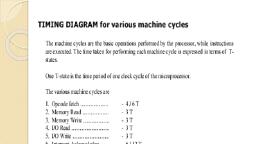
Cycles and States, From the above discussion, we can define terms that will become handy later on:, T- State:, One subdivision of an operation performed in one clock period., Each T states is precisely equal to one clock period., An instruction’s execution length is usually measured in a number of T-states., , Machine Cycle:, The time required to complete one operation of accessing memory, I/O, or, acknowledging an external request., This cycle may consist of 3 to 6 T-states., Various machine cycle in 8085 is, , , , , , , , Opcode fetch, Memory read/write, Input read/write, Intereupt acknowledge, Halt/hold, Reset, , Instruction Cycle:, The time required to complete the execution of an instruction., In the 8085, an instruction cycle may consist of 1 to 6 machine cycles.
Page 78 :
Processor Cycle, The function of the microprocessor is divided into two cycle of the instruction, Fetch, Execute, Number of instructions are stored in the memory in sequence., In the normal process of operation, the microprocessor fetches (receives or reads) and, executes one instruction at a time in the sequence until it executes the halt (HLT), instruction., , Thus, an instruction cycle is defined as the time required to fetch and execute an, instruction., Instruction Cycle (IC) = Fetch cycle (FC) + Execute Cycle (EC), , Processor Cycle
Page 79 :
Instruction cycle, , Machine cycle1, , T – State 1, , T – State 2, , Machine cycle 2, , T – State 3, , Machine cycle 5, , T – State 6
Page 80 :
The 8085 microprocessor has 7 basic machine cycles., They are, 1. Opcode fetch cycle (4T), 2. Memory read cycle or operand fetch(3 T), 3. Memory write cycle (3 T), 4. I/O read cycle (3 T), 5. I/O write cycle (3 T), 6. Interrupt Acknowledge, 7. Bus Idle cycle
Page 81 :
Opcode Fetch Machine Cycle, The first step of executing any instruction is the Opcode fetch cycle., In this cycle, the microprocessor brings in the instruction’s Opcode, from memory., To differentiate this machine cycle from the very similar “memory, read” cycle, the control & status signals are set as follows:, IO/M=0(memory operation),, s1 and s0 are both 1. (opcode fetch), This machine cycle has four T-states., The 8085 uses the first 3 T-states to fetch the opcode., T4 is used to decode and execute it., It is also possible for an instruction to have 6 T-states in an opcode fetch, machine cycle.
Page 82 :
Timing Diagram of Opcode Fetch, , Timing Diagram for Opcode Fetch Machine Cycle
Page 83 :
Timing: Transfer of byte from memory to MPU, How a data byte is transfer from, , memory to the MPU., It shows the five different group of, signals with clock, , Step 1: At T1 higher order memory, address 20H is placed on the A15 – A8, and the lower order memory address, 05H is placed on the bus AD7-AD0, and, ALE signal high. IO/M goes low(memory, related signal)., Step 2: During T2 RD signal is sent out., RD is active during two clock periods., Step 3 : During T3, Memory is enabled then instruction byte 4FH is placed on the data, bus and transferred to MPU. When RD goes high it causes the bus to go into high, impedance state., Step 4: During T4, the machine code or byte is decoded by the instruction decoder and, content of A is copied into register.
Page 84 :
Data Flow, form, Memory to, MP, , 85
Page 85 :
Memory Read or Operand Fetch Machine Cycle, This cycle is executed by the processor to read a data byte from, memory or to fetch operand in a multi byte instruction. For ex. 2 or 3, byte instruction because in 1 byte instruction the machine code is an, opcode; so operation is always an opcode fetch, The instructions which have more than one byte word size will use, the machine cycle after the opcode fetch machine cycle., , The memory read machine cycle is exactly the same as the, opcode fetch except:, , , , , , IO/M= 0(memory operation),, s1 = 1 and s0 = 0. (memory read), WR = 1 & RD = 0, It only has 3 T-states, , First cycle is opcode fetch cycle., So this cycle requires, 4T(opcode) +3T(memory read )=7 T states to execute.
Page 86 :
Timing Diagram of Memory Read Machine Cycle
Page 87 :
Timing for execution of the instruction MVI A, 32H, MVIA, 32H is 2 byte instruction, so hex code for MVI A is 3E., 8085 decode the opcode and finds out a second byte need to be read, , High Impedance state.
Page 88 :
The execution times of the memory read machine cycle and the instruction, cycle are calculated as, Clock Frequency f = 2MHz, T state = clock period (1/f ) = 0.5µsec, Execution time for opcode fetch = 4T * 0.5 = 2µsec, Execution time for Memory Read = 3T * 0.5 = 1.5µsec, Execution time for Instruction = 7T * 0.5 = 3.5µsec, , 88
Page 89 :
Data Flow, form, Memory to, MP, , 89
Page 90 :
Memory Write Machine Cycle, The memory write machine cycle is executed by the processor, to write a data byte in a memory location., The memory write machine cycle is exactly the same as the, memory read except:, IO/M= 0(memory operation),, s1 = 0 and s0 = 1. (memory read, WR = 0 & RD = 1, It only has 3 T-states, , First cycle is opcode fetch cycle., So this cycle requires, 4T(opcode) +3T(memory write )=7 T states to execute.
Page 91 :
Timing Diagram of Memory write Machine Cycle
Page 92 :
Data Flow, form MPU, to Memory, , 93
Page 93 :
Input/ Output Read Machine Cycle, Microprocessor executes this cycle to read content of I/O port, or to read 8 bit data present on an input ports through data bus., The I/O read machine cycle is exactly the same as the memory, read except:, IO/M= 1(I/O operation),, s0 = 0 and s1 = 1. ( read), WR = 1 & RD = 0, It only has 3 T-states, , This instruction reads the data from an input device and places, the data byte in the accumulator., It accept the data from input device by using I/O read, signal(IOR).
Page 94 :
Timing Diagram of I/O read Machine Cycle
Page 95 :
Data Flow, form input, device to MP, , 96
Page 96 :
Input/output write Machine Cycle, Microprocessor executes this cycle to write a data into an I/O, port or to write 8 bit data present on an output ports., The I/O write machine cycle is exactly the same as the memory, write except:, IO/M= 1(I/O operation),, s1 = 1 and s0 = 0. ( write), WR = 0 & RD = 1, It only has 3 T-states, , This instruction places the content of the accumulator on the, data bus., It transmit the data to output device by using I/O write, signal(IOW).
Page 97 :
Timing Diagram of I/O write Machine Cycle
Page 98 :
Data Flow, form MPU to, output, device, , 99
Page 99 :
Interrupt Acknowledge Cycle, Interrupt is hardware call of subroutine., MPU executes this cycle to acknowledge INTR request, MPU determines the starting address of the interrupt service, routine by using interrupt information., RSTn and CALL address is used as interrupt information., Length of this cycle is 6T or 3T states., So two interrupt acknowledge cycle, (A) Interrupt acknowledge of RSTn, (B) Interrupt acknowledge of CALL address
Page 100 :
Interrupt Acknowledge of RSTn, The RSTn instruction is one byte., It is similar to opcode fetch cycle with, INTA signal is activated instead of RD signal., IO/M= 1(I/O operation),, s0 = 1 and s1 = 1., It only has 6 T-states
Page 101 :
Timing Diagram of Restart instruction
Page 102 :
Interrupt Acknowledge for CALL, The CALL instruction is Three byte. So MPU executes 3, interrupt acknowledge cycle., The length of the first cycle is 6 T states while second and third, cycle is 3T states., PC is not incremented. IR is selected as destination register, during 1st interrupt acknowledge cycle and in 2nd and 3rd cycle Z, and W are selected as destination register, It is similar to opcode fetch cycle with, IO/M= 1(I/O operation),, s0 = 1 and s1 = 1.
Page 103 :
Timing Diagram of CALL instruction
Page 104 :
Bus Idle Cycle, The MPU executes this cycle for internal operation. Few, situations where the machine cycle are neither read nor write., For Execution of DAD instruction: this instruction add the content of a specified register pair to the, content of HL pair., After opcode fetch, DAD requires extra 6 T states to add 16 bit, content ., This extra T states are divided into two machine cycle do not involve, any memory or I/O operation., , During Internal Opcode generation(For TRAP and RST) –, In response to TRAP interrupt, 8085 enters into a bus idle cycle, during which it invokes restart instruction, stores the content of, PC onto the stack and places 0024H on the PC.
Page 105 :
Timing Diagram of DAD instruction
Page 106 :
Timing Diagram of DAD instruction
Page 107 :
Bus Idle cycle for TRAP
Page 108 :
WAIT State, When speed of memory system and I/O system are not, compatible with MPU timings, means longer time for read/, write data., So MPU has to confirm whether a peripheral is to ready transfer, data op not, If READY pin s high the peripheral is ready. Otherwise it is, continue as long as READY is low., During the wait state the content of the address bus, the data, bus and control bus are held constant., The wait state gives an I/O port an extra clock time to output, valid data on the data bus.
Page 109 :
Read Machine cycle with and without wait state
Page 110 :
Introduction to 8085 based micro-computer