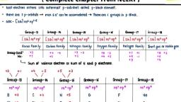
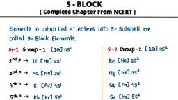
Page 1 :
THE SOLID STATE, , 1
Page 2 :
CONTENTS, , ➢ Types of solids, , ➢ Types of structures adopted by solids, ➢Imperfections in solids, , Dr. K.S. VIKAS, , 2
Page 3 :
SOLIDS can be divided into two categories., , ➢ Crystalline, , ➢ Amorphous, Crystalline has long range order, , Amorphous materials have short range order, , 3
Page 4 :
Types of Solids, • Crystalline solid: well-ordered, definite arrangements of, molecules, atoms or ions., •, •, •, •, , Crystals have an ordered, repeated structure., sharp melting point, Anisotropy, True solids, , • Amorphous solid: no definite arrangement of molecules,, atoms, or ions (i.e., lack well-defined structures or, shapes)., • Amorphous solids vary in their melting points., • Isotropy, • Pseudo solids (super cooled liquids), Dr. K.S. VIKAS, , 4
Page 6 :
STRUCTURE AND TYPES OF, CRYSTALLINE SOLIDS, Na+, Cl-, , Molecular Solids, , Covalent Solids, , Ionic solids, , Metallic solids, Dr. K.S. VIKAS, , 6
Page 7 :
Types of Crystalline Solids, 1. Molecular Solids, • Lattice points occupied by molecules, • Held together by intermolecular forces like, London forces, dipole-dipole force or hydrogen, bonding, • Soft, low melting point, • Poor conductor of heat and electricity, , Dr. K.S. VIKAS, , 7
Page 8 :
Types of Crystalline Solids, 2. Ionic Solids, • Lattice points occupied by cations and anions, • Held together by electrostatic attraction, • Hard, brittle, high melting point, • Poor conductor of heat and electricity, , CsCl, , ZnS, Dr. K.S. VIKAS, , CaF2, 8
Page 9 :
Types of Crystalline Solids, 3. Covalent Solids, • Lattice points occupied by atoms, • Held together by covalent bonds, • Hard, high melting point, • Poor conductor of heat and electricity, , carbon, atoms, , graphite, , diamond, Dr. K.S. VIKAS, , 9
Page 10 :
Types of Crystalline Solids, 4. Metallic Solids, • Lattice points occupied by positive metal ions, • Held together by metallic bonds, • Soft to hard, low to high melting point, • Good conductors of heat and electricity, Cross Section of a Metallic Crystal, nucleus &, inner shell e-, , mobile “sea”, of e-, , Dr. K.S. VIKAS, , 10
Page 11 :
TYPES OF CRYSTALLINE SOLIDS, Crystal, Type, , Particles, , Interparticle Physical Behaviour, Forces, , Molecular, , Molecules, , Ionic, , Positive, and, negative, ions, , Dispersion, Dipoledipole, H-bonds, Electrostatic, attraction, , Covalent, or Network, , Atoms, , Covalent, , Metallic, , Positive, metal ions, , Metallic, bond, , Dr. K.S. VIKAS, , ➢ Fairly soft, ➢ Low to moderate mp, ➢ Poor thermal and electrical, conductors, ❑Hard and brittle, ❖ High mp, ❖ Good thermal and electrical, conductors, in, molten, condition, • Very hard, • Very high mp, • Poor thermal and electrical, conductors, ❑ Soft to hard, ❑ Low to very high mp, ❑ Mellable and ductile, ❑ Excellent thermal and, electrical conductors, , Examples, O2, P4, H2O,, Sucrose, , NaCl, CaF2,, MgO, , SiO2(Quartz), C (Diamond), Na, Cu, Fe, , 11
Page 12 :
CRYSTAL STRUCTURE, Cristal Lattice: Crystal Lattice is the arrangement of points in, three dimensional space, representing constituent particles in a, crystal., Space Lattice Arrangements of atoms, = Lattice of points onto which the atoms are hung., , •, •, •, , •, •, •, , •, •, •, , =, +, , Space Lattice + Basis = Crystal Structure, Elemental solids (Argon): Basis = single atom., Polyatomic Elements: Basis = two or four atoms., Complex organic compounds: Basis = thousands of atoms., Dr. K.S. VIKAS, , 12
Page 13 :
Definitions, 1. The unit cell, “The smallest repeat unit of a crystal structure,, which when repeats in all the three dimensions to, form the crystal”, The unit cell is a box with:, , • 3 sides - a, b, c, , • 3 angles - , , , , Dr. K.S. VIKAS, , 13
Page 14 :
Structures of Solids, Unit Cells, , The smallest repeating unit that shows, the symmetry of the pattern is called the, unit cell., Dr. K.S. VIKAS, , 14
Page 16 :
LATTICE TYPES, , Primitive ( P ), , Face Centered ( F ), , Body Centered ( I ), , End-Centered (C ), , 16
Page 17 :
Lattices, , Auguste Bravais, (1811-1863), , In 1848, Auguste Bravais demonstrated, , that in a 3-dimensional system there are, fourteen possible lattices, A Bravais lattice is an infinite array of, discrete points with identical environment, seven crystal systems + four lattice, centering types = 14 Bravais lattices, , 17
Page 18 :
BRAVAIS LATTICES, , 7 UNIT CELL TYPES + 4, LATTICE TYPES = 14, , BRAVAIS LATTICES, , Dr. K.S. VIKAS, , 18
Page 19 :
Common Types of Cubic Unit Cells, • Three common types of Cubic unit cell., , • Primitive cubic, atoms at the corners of a simple cube, – each atom shared by 8 unit cells;, , • Body-centered cubic (bcc), atoms at the corners of a, cube plus one in the center of the body of the cube,, – corner atoms shared by 8 unit cells, center atom completely, enclosed in one unit cell;, , • Face-centered cubic (fcc), atoms at the corners of a, cube plus one atom in the center of each face of the cube,, – corner atoms shared by 8 unit cells, face atoms shared by 2, unit cells., Dr. K.S. VIKAS, , 19
Page 21 :
Shared by 2 unit cells, , Shared by 8 unit cells, , Dr. K.S. VIKAS, , 21
Page 22 :
Unit Cells, , Dr. K.S. VIKAS, , 22
Page 23 :
Table showing Atom Fractions, in Unit Cells, Position in the, Unit Cell, Corner, , Fraction in the, unit cell, 1/8, , Body Centre, , 1, , Face Centre, , 1/2, , Dr. K.S. VIKAS, , 23
Page 24 :
Number of Atoms in a Unit Cell, , 1 atom/unit cell, , 2 atoms/unit cell, , 4 atoms/unit cell, , (8 x 1/8 = 1), , (8 x 1/8 + 1 = 2), , (8 x 1/8 + 6 x 1/2 = 4), , Dr. K.S. VIKAS, , 24
Page 25 :
CLOSE-PACKING OF SPHERES, , Dr. K.S. VIKAS, , 25
Page 26 :
CLOSE-PACKING IN TWO DIMENSIONS, , SQUARE PACKING, , HEXAGONALCLOSE PACKING, , AAA…. Type, , ABAB…. Type, , Each particle in contact with, 4 others, , Each particle in contact with, , Dr. K.S. VIKAS, , 6 others, , 26
Page 27 :
TWO LAYERS PACKING, , Dr. K.S. VIKAS, , 27
Page 28 :
THREE LAYERS PACKING, , Dr. K.S. VIKAS, , 28
Page 30 :
Hexagonal close packing, , Dr. K.S. VIKAS, , Cubic close packing, , 30
Page 31 :
Packing Efficiency, volume of sphere, Packing Efficiency =---------------------------- X 100, Total volume of cube, (N)x (4/3 Π r3), = --------------------- X100, a3, , Dr. K.S. VIKAS, , 31
Page 36 :
NON-CLOSE-PACKED STRUCTURES, a) Body centered cubic ( BCC ) b) Primitive cubic ( P), , 68% of space is occupied, Coordination number = 8, , Dr. K.S. VIKAS, , 52% of space is occupied, Coordination number = 6, , 36
Page 37 :
Face-Centered Cubic Crystal Structure, , 68% of space is occupied, Hexagonal close packing &, Cubic close packing also, occupy the same space, , Dr. K.S. VIKAS
Page 39 :
TYPE OF HOLES IN CLOSE PACKING, , TETRAHEDRAL HOLES, , OCTAHEDRAL HOLES, , Dr. K.S. VIKAS, , 39
Page 40 :
Imperfections in Solids, or, crystal defects
Page 41 :
Crystal Defects, • Perfect crystals do not exist; even the best crystals have, , defects., – defects are imperfections in the regular repeating, , pattern, – Point defect, – Line defect, , 1. Point Defects, A.Vacancies, – given a perfect crystal (e.g. of Cu), an atom can be placed, on the outside of the cell to produce a vacancy (≡ □)., , Dr. K.S. VIKAS, , 41
Page 44 :
1. Stoichiometric Defects, 1) Shottky Defect, – equal numbers, of anion and cation vacancies., – may be randomly distributed, but tend, to cluster because of oppositely charged, vacancies., – most important with alkali halides., , Dr. K.S. VIKAS, , 44
Page 45 :
2) Frenkel Defect, Dislocation of cation, cation occupies, interstitial position (void, between normal atomic, position)., , Dr. K.S. VIKAS, , 45
Page 46 :
Non-stoichiometric Defects, Metal excess defect, anion vacancies, excess cation, Metal deficiency defect, cation vacancies
Page 47 :
Metal excess, defect, Anion vacancies, An anion is missing from the, crystal lattice and that place, is occupied by an electron, Color Centers (F-center; Ger:, farbenzentre), Dr. K.S. VIKAS, , 47
Page 48 :
Excess cation: in interstitial places
Page 49 :
Metal deficiency defect cation, vacancies
Page 50 :
3. Impurity defect
Page 51 :
Electrical Properties
Page 52 :
Conductors, Insulators, Semiconductors, , 52
Page 53 :
Energy Gap, , Energy (Eg) required to promote electrons from the valence band to the, conduction band.
Page 54 :
Insulators, electrons to move throughout, the material., Inter-atomic bonding is ionic or, strongly covalent. The valence, electrons are tightly bonded,, highly localized and not free to, scatter throughout the crystal., The band-gap is large, the, valence band is full, and the, conduction band is empty., , • Insulators:, , -- wide band gap (> 2 eV), -- few electrons excited, across band gap, , Energy, , empty, conduction, band, GAP, , filled states, , In insulators there are no free, , filled, valence, band, filled, band, 54
Page 55 :
Semiconductors, , ❑, , ❑, , In semiconductors,, bonding is, predominantly covalent, (relatively weak)., These electrons are, more easily removed by, thermal excitation., The band-gap is, smaller, the valence, band is full, and the, conduction band is, empty., , •, , Semiconductors:, -- narrow band gap (< 2 eV), -- more electrons excited, across band gap, empty, conduction, band, , ?, , GAP, , Energy, filled states, , ❑, , filled, valence, band, filled, band, 55
Page 56 :
Conductors, -- for metals, empty energy states are adjacent to filled states., , - partially filled band, - empty band that, overlaps filled band, , Energy, , Overlapping bands, Energy, , empty, band, empty, band, , GAP, , partly, filled, band, , filled, band, , filled states, , • two types of band, structures for metals, , Partially filled band, , filled states, , • thermal energy, excites electrons, into empty higher, energy states., , filled, band, , filled, band, 56
Page 57 :
Semiconductors, Intrinsic semiconductors, Extrinsic Semiconductors
Page 58 :
Intrinsic Semiconductor, materials, Silicon and germanium each, , have 4 electrons in their outer, orbital. This allows them to, form crystals., In a silicon lattice, all silicon, atoms covalently bond to 4, neighbors, leaving no free, electrons to conduct electric, current. This makes a silicon, crystal an insulator rather than, a conductor., , A chip, an LED and a, transistor are all made, from semiconductor, material.
Page 59 :
Intrinsic Semiconductor, On heating some of the covalent bonds, , between silicon atoms are broken and as a, result they conduct electricity, Semiconductors in the pure form is called, , intrinsic semiconductors
Page 60 :
Extrinsic semiconductors, They contain some suitable impurities in their crystal, , lattice. This process of adding impurities to the crystal, is called doping . They are classified into two based on, the impurity present in it., ➢ n-type semiconductor, ➢ p-type semiconductor
Page 61 :
Doping Silicon to Create n-Type, Silicon, The "dopant” has 5 valence electrons;, , silicon has 4., Substituting a phosphorus atom with, 5 valence electrons for a silicon atom, in a silicon crystal leaves an extra,, unbonded electron that is relatively, free to move around the crystal.
Page 62 :
Doping Silicon to Create p-Type, Silicon, The "dopant” has 5 valence, , electrons; silicon has 4., Substituting a boron atom, with 3 valence electrons for a, silicon atom in a silicon, crystal leaves a hole (a bond, missing an electron) that is, relatively free to move around, the crystal.
Page 63 :
When a dopant atom with a valence of less than four is substituted, into the silicon structure, a hole is created in the structure and an, acceptor energy level is created just above the valence band. Little, energy is required to excite the holes into motion.
Page 65 :
Diamagnetism, Diamagnetic materials tend, , to repel flux lines weakly, All the electrons are paired, They lose their magnetism in, the absence of external, magnetic field., , Examples: water, protein, fat
Page 66 :
Paramagnetism, Paramagnetic substances are attracted weakly by a, , magnetic field., They lose their magnetism in the absence of external, magnetic field., They have one or more unpaired electrons., E.g. O2, Cu2+, Fe3+, Cr3+
Page 67 :
Ferromagnetism, Materials that retain a, , magnetization in zero field, They are attracted strongly, by a magnetic field, They have more unpaired, electrons., Examples: iron, cobalt
Page 68 :
Antiferromagnetism, They are expected to be, , ferromagnetic but shows, zero magnetic moment., The magnetic moments are, , oppositely arranged and, hence cancel each other., Many metal oxides are, , antiferromagnetic
Page 69 :
Ferrimagnetism, They are expected to be, ferromagnetic but shows only, small magnetic moment., The magnetic moments are, oppositely arranged but all, magnetic moments are not, canceled., , E.g. Fe2O3