Page 1 :
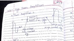
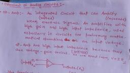
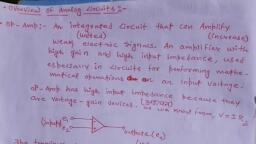
Chapter 8, Integrated circuits, 8.1 Introduction, An integrated circuit (IC) is an electronic circuit consisting of large number of, electronic devices such as resistors, capacitors, diodes, transistors, ete. are fab-, ricated on a single)semiconductor substrate. It is also called achip) Introduction, of integrated circuits made electronic devices with very small size combined, with a lot of functions in a single device. AnIC can function as an amplifier,, oscillator, computer memory, etc. ), Integrated circuits can be classified as analog ICs and digital ICs. Analog, ICs are also known as linear ICs. They havecontinuously variable output that, depends on the input signal amplitude As the term implies, the output signal is, a linear function of the input. The operational amplifier (op-amp) is a common, device in these applications. IC 741 is one of widely used op-amp., Digital ICs operate at only a few defined levels or states, rather than over, a continuous range of signal amplitudes. These devices are used in computers,, switching circuits, etc.)The fundamental building blocks of digital ICs are logic, gates, which operate with binary data, that is, signals that have only two different, states, called low (logic 0) and high (logic 1)., The advantages of integrated circuits are, 1. Very small size and low weight, 2. Reduced cost, 3. High reliability, 4. Low power requirement, 5. Easy replacement, 152, 1
Page 2 :
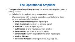
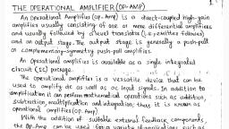
ean erasing, 8.2 The operational amplifier, An operational amplifier is a direct coupled high gain amplifier consisting of, one or more differential amplifiers and followed by a level shifting circuit and, an output stage. An operational amplifier is available as a single integrated, circuit package. The block diagram of op amp is shown in the Figure 8.1., Non inverting, input, Level, Input, Stage, Intermediate, Stage, Shifting, Circuit, Output, Stage, Output, Inverting, input, Figure 8.1: Block diagram of op amp, The input stage is a dual input balanced output differential amplifier) (It, means the differential amplifier has two inputs and an output taken between, two output points).(This stage provides most of the voltage gain of the amplifier, and also establishes the input resistance of the op amp. The intermediate stage, of op amp is another differential amplifier which is driven by the output of the, first stage. This is usually dual input unbalanced output It means that the output, is taken with respect to ground point)., Because direct coupling is used, the de voltage level at the output of inter--, mediate stage is well above ground potential. Therefore, (evel shifting cireuit is, used to shift the de level at the output downward to zero with respect to ground., (The output stage is generally a push pull complementary amplifier. The out-, put stage increases the output voltage swing and raises the current supplying, capability of the op amp. It also provides low output resistance., The symbolic diagram of an op amp is shown in Figure 8.2. 741C is the, most commonly used op amp available in IC package. It is an 8-pin DIP (Dual, in Line Package) chip. Pinout of 741C IC is shown in Figure 8.3., The ideal op-amp, An ideal op-amp will exhibit the following characteristics., 1. Infinite voltage gain., 2. Infinite input resistance.)so that almost any signal source can drive it and, there is no loading of the input source., 153, 2
Page 3 :
154, Integrated circuits, + de supply, V+, voltage, Inverting, Input (-Vin), Output, Non inverting, Input (+Vin), - de supply, voltage, V-, Figure 8,2: Symbolic diagram of t, op-amp, Offsct || 1, 8|| NC, -Vin, 2, V+, 3., +Vin, Output, V- 14, 5 Ofiset, 741, Figure 8.3: Pin out of 741C, op-amp, 3. Zero output resistance, so that output can drive an infinite number of other, devices., 4. Infinite bandwidth so that any signal frequency from zero to infinity can, be amplified without attenuation., 5. Infinite common mode rejection ratio so that the, noise voltage is zero., fuput, common mode, 6. Infinite slew rate, so that output voltage changes occur simultaneously, with input voltage changes., 7. Zero output voltage when input voltage is zero., Equivalent circuit of op-amp, Figure 8.4 shows an equivalent circuit of an op-amp. Vị and V2 are the two input, voltages. Ri is the input resistance of op-amp and Aa is the voltage gain of op-, amp. AdVa is an equivalent voltage source and Ro is the equivalent resistance, found when looking back into the terminal of an op-amp., This equivalent circuit is useful in analyzing the basic operating principles, 154, 3
Page 4 :
The operational amplifier, 155, of op-amp and in observing the effects of standard feedback arrangements., V. = Ad(Vi – V2) = Ad x Va, -, This equation indicates thatthe output voltage V. is directly proportional, to the algebraic difference between the two input voltages.) In other words the, op-amp amplifies the difference between the two input voltages. The polarity of, the output voltage depends on the polarity of the difference voltage Va., Vi, Ro, V Ri, AdVe, o Vo, V2 0=, Figure 8.4: Equivalent circuit of op-amp, 8.2.3 Parameters of op-amp, The various important parameters of op-amp are the following., Vio = 2 mv, Input Offset Voltage, Input offset voltage Vio is defined as the voltage that must be applied between, the two input terminals of an op-amp to nullify the output. ) It may be either, positive or negative. For a 741C op-amp the typical value of Vio is 2 mV., Input offset Current 0 2oonA, The input offset current Iio is the difference between the currents into inverting, and non-inverting terminals of a balanced amplifier.), Iio = |IB1 – IB2|, %3D, The Iio for the 741C is 200 A maximum., hput Bias Current, he input bias current Ig is the average of the current, entering the input termi-, 155, 4
Page 5 :
156, Integrated circuits, nals of an op-amp., IB1 + IB2, IB, For 741C, IB(maa), 700 nA, Differential Input Resistance (R;), Differential iuput resistance Ri is the equivalent resistance that can be measured, at either the inverting or non-inverting input terminal with the other terminal, grounded.) For the 741C, the input resistance is relatively high (2 MS2)., Common Mode Rejection Ratio (CMRR), CMRR is defined as the ratio of the differential voltage gain Ad to the common, mode voltage gain Aem., Ad, Acm, CMRR, Ad, CMRR in dB = 20log, Acm, For the 741C, CMRR is 90 dB typically( The higher the value of CMRR the, better is the matching between two input terninals and the smaller is the output, common mode voltage.), Supply Voltage Rejection Ratio (SVRR), (SVRR is the ratio of the change in the input offset voltage to the corresponding, change in power supply voltages. i.e.,, SV RR = AVio/AV, It is expressed in uV/V or in decibels., ( Where AV is the change in the input supply voltage and AVio is the corre-, sponding change in the offset voltage. For the 741C, SV RR 150 µV/V., Voltage Gain, Since(the op-amp amplifies difference of the voltages at two input terminals, the, voltage gain of the amplifier is defined as, Output voltage, Differential input voltage, Voltage gain, Because output signal amplitude is much larger than the input signal, voltage gain is commonly called large signal voltage gain. Typical voltage, 156, 5