Page 1 :
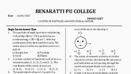
BENAKATTI PU COLLEGE, , Date : 01/08/2022, TEST ID: 1709, Time : 01:00:00 Hrs., KCET, PU-II-PHYSICS, Marks : 60, 14.SEMICONDUCTOR ELECTRONICS: MATERIALS,DEVIES AND SIMPLE CIRCUITS, Single Correct Answer Type, 1. Barrier potential of a p-n junction diode does, not depend on, a) Forward bias, b) Doping density, c) Diode design, d) Temperature, 2. Within depletion region of p-n junction diode, a) 𝑝-side is positive and 𝑛-side is negative, b) 𝑝-side is negative and 𝑛-side is positive, c) Both sides are positive or both negative, d) Both side are neutral, 3. In the middle of the depletion layer of reverse, biased p-n junction, the, a) Electric field is zero, b) Potential is maximum, c) Electric field is maximum, d) Potential is zero, 4. Which of the energy band diagrams shown in, the figure corresponds to that of a, semiconductor?, a), b), , reverse biased?, a), , R, + 5 V, , b), , 5., , 6., , 7., , 8., , d), , The temperature coefficient of a zener, mechanism is, a) Negative, b) Positive, c) Infinity, d) Zero, Energy gap between valence band and, conduction band of a semiconductor is, a) Zero, b) Infinite c) 1 eV, d) 10 eV, In silicon when phosphorus is doped ……. is, formed, a) 𝑝-type semiconductor, b) 𝑛-type semiconductor, c) p-n junction, d) None of these, In the following, which one of the diodes is, , -12 V, , R, , - 10 V, , c), R, , - 10 V, , d), , + 5 V, , R, , 9., , 10., , 11., , c), , + 10 V, , 12., , 13., , 14., , 15., , If a full wave rectifier circuit is operating from, 50Hz mains, the fundamental frequency in the, ripple will be, a) 70.7 Hz b) 100 Hz c) 25 Hz d) 59 Hz, The 𝑛-type semiconductors are obtained, when, germanium is doped with, a) Arsenic, b) Phosphorus, c) Antimony, d) Any one of these, In order to prepare a 𝑝-type semiconductor,, pure silicon can be doped with, a) Phosphorus, b) Aluminium, c) Antimony, d) Germanium, In an 𝑛-type semiconductor, the fermi energy, level lies, a) In the forbidden energy gap nearer to the, conduction band, b) In the forbidden energy gap nearer to the, valence band, c) In the middle of forbidden energy gap, d) Outside the forbidden energy gap, A zener diode is used for, a) Rectification, b) Modulation, c) Detection, d) Voltage regulation, The depletion layer in a silicon diode is 1 𝜇m, wide and its knee potential is 0.6 V, then the, electric field in the depletion layer will be, a) 0.6 Vm−1, b) 6 × 10⁴ Vm−1, d) Zero, c) 6 × 10⁵ Vm−1, Doping of intrinsic semiconductor is done, a) To neutralize charge carriers, b) To increase the concentration of majority, Page|1
Page 2 :
charge carriers, c) To make it neutral before disposal, d) To carry out further purification, 16. In a reverse biased diode when the applied, voltage changes by 1 V, the current is found to, change by 0.5 𝜇A. The reverse bias resistance, of the diode is, a) 2 × 10⁵ Ω, b) 2 × 10⁶ Ω, c) 200 Ω, d) 2 Ω, 17. In a forward biased p-n junction diode, the, potential barrier in the depletion region is of, the form, a), V, , P, , b), , n, , V, , P, , c), , n, , V, , P, , d), , n, , V, , d), , 21. Which of the following statements is not, correct when a junction diode is in forward, bias?, a) The width of depletion region decreases., Free electrons on 𝑛-side will move towards, b), the junction., c) Holes on 𝑝-side move towards the junction., Electrons on 𝑛-side and holes on 𝑝-side will, d), move away from junction., 22. The potential in depletion layer is due to, a) Electrons, b) Holes, c) Ions, d) Forbidden band, 23. When a 𝑝-𝑛 junction diode is reverse biased,, then, a) No current flows, b) The depletion region is increased, c) The depletion region is reduced, d) The height of the potential barrier is reduced, 24. In the circuit, if the forward voltage drop for, the diode is 0.5 V, the current will be, 0.5 V, , P, , n, , 18. 𝑛-type semiconductor is, a) Positively charged, b) Negatively charged, c) Neutral, d) Positive or negative depending upon doping, material, 19. When boron is added as an impurity to silicon,, the resulting material is, a) n-type semiconductor, b) n-type conductor, c) p-type conductor, d) p-type semiconductor, 20. The output wave form of full-wave rectifier is, a), , 8 V, , 25., , 26., , 27., , b), 28., c), , 2.2 K, , a) 3.4 mA b) 2 mA, c) 2.5 mA d) 3 mA, What is the name of the level formed due to, impurity atom in 𝑝-type in the forbidden gap?, a) Donor level, b) Acceptor level, c) Conduction level, d) Forbidden level, At absolute zero, Si acts as, a) Non-metal, b) Metal, c) Insulator, d) None of these, Which of the following statements is true for, an 𝑛-type semiconductor?, a) The donor level lies closely below the, bottom of the conduction band., b) The donor level lies closely above the top of, the valence band, c) The donor level lies at the halfway mark of, the forbidden energy gap, d) None of the above, If in a p-n junction diode, a square input signal, of 10 V is applied as shown, 5V, , RL, , -5 V, , Page|2
Page 3 :
Then the output signal across 𝑅𝐿 will be, 10 V, a), b), , a), , -10 V, , c), , d), , b), , +5 V, , -5 V, , 29. Frequency of given AC signal is 50 Hz. When it, is connected to a half-wave rectifier, the, number of output pulses given by rectifier, within 1 s is, a) 50, b) 100, c) 25, d) 150, 30. The energy gap between conduction band and, the valence band is of the order of 0.7 eV. Then, it is, a) An insulator, b) A conductor, c) A semiconductor, d) An alloy, 31. In LED visible light is produced by, a) Gallium phosphide, b) Gallium arsenide, c) Germanium phosphide, d) Silicon phosphide, 32. The depletion layer of a p-n junction, a) Is of constant width irrespective of the bias, b) Acts like an insulating zone under reverse, bias, c) Has a width that increases with an increase, in forward bias, d) Is depleted of ions, 33. Name of a 𝑝-𝑛 junction, which can be used as, the regulator, is, a) Zener diode, b) Tunnel diode, c) Gunn diode, d) None of these, 34. A reverse biased diode is, -6 V, -3 V, a), b), , 3 V, , c), , 0V, , d), , c), , d), , 37. Electric conduction in semi-conductor takes, place due to, a) Electrons only, b) Holes only, c) Both electrons and holes, d) None of the above, 38. In the case of forward biasing of a p-n junction, diode, which one of the following figures, correctly depicts the direction of conventional, current (indicated by an arrow mark)?, a), - +, P, , b), P, , -, , +, , -, , +, +, , n, , n, , - +, , 2 V, , 2 V, , +, +, , -, , c), , -2 V, , -, , P, , 35. The current in the circuit shown in the figure,, considering ideal diode is, , - +, - +, , n, , 100, 3.2 V, , 3 V, , a) 20 A, b) 2 × 10⁻³ A, c) 200 A, d) 2 × 10⁻⁴ A, 36. Which is the correct diagram of a half-wave, rectifier?, , d), P, , -, , +, , -, , +, +, , -, , n, , 39. By increasing the temperature, the specific, Page|3
Page 4 :
resistance of a conductor and a semiconductor, a) Increases for both, b) Decreases for both, c) Increases, decreases respectively, d) Decreases, increases respectively, 40. The energy gap of silicon is 1.14 eV. At what, wavelength the silicon will stop to absorb the, photon?, a) 10877 Å b) 9888 Å c) 1087.7 Åd) 1000 Å, 41. A p-n junction (𝐷) shown in the figure can act, as a rectifier. An alternating current source (𝑉), is connected in the circuit., D, V, , R, , a), , a) NOT, b) AND, c) OR, d) NAND, 44. When the two inputs of a NAND gate are, shorted, the resulting gate is, a) NOR, b) OR, c) NOT, d) AND, 45. A logic gate and its truth table are shown, below, , 𝑨, 𝑩, 𝒀, 0, 0, 0, 0, 1, 1, 1, 0, 1, 1, 1, 1, The gate is, a) NOR, b) AND, c) OR, d) NOT, 46. The output of given logic circuit is, , b), a) A + B + C, c) A ∙ (B ∙ C), 47. Output 𝑌 is given by, , b) (A + B) ∙ (A + C), d) A ∙ (B + C), , c), , d), a) (𝑋 ∙ 𝑌) ∙ 𝑍, , 42. In a 𝑝-𝑛 junction diode, a square input signal of, 10 V is applied as shown in figure. The output, signal across 𝑅𝐿 will be, R, , 5 V, , L, , - 5 V, , a), , 10 V, , b), 5V, , c), , -5 V, , d), , -10 V, , 43. Which type of gate the following truth table, represents?, 𝐈𝐧𝐩𝐮𝐭𝐬, 𝑨, 0, 0, 1, 1, , 𝑩, 0, 1, 0, 1, , b) (𝑋 + 𝑌) 𝑍, , c) (𝑋 + 𝑌) 𝑍, d) 𝑋 ∙ 𝑌 + 𝑍, 48. Identify the true statement for OR gate, Output 𝑌 will be 1 when input 𝐴 or 𝐵 or both, a), are 1, Output 𝑌 will be 0 when the either of the, b), inputs 𝐴 or 𝐵 is 1, Output 𝑌 will be 1 only when both the inputs, c), 𝐴 and 𝐵 are 1, Output 𝑌 will be 1 only when either of the, d), inputs 𝐴 and 𝐵 are 1, 49. To get an output 𝑌 =1 from the circuit shown,, the inputs 𝐴, 𝐵 and 𝐶 must be respectively, , 𝐎𝐮𝐭𝐩𝐮𝐭, a) 0, 1, 0 b) 1, 0, 0 c) 1, 0, 1 d) 1, 1, 0, 𝑸, 150. The circuit shown in the figure contains two, 1, diodes each with a forward resistance of 50 Ω, 1, and with infinite backward resistance. If the, 0, battery is 6 V, the current through the 100 Ω, Page|4
Page 5 :
resistance (in ampere) is, 150 Ω, 50 Ω, 6V, , 51., , 52., , 53., , 54., , 55., , 100 Ω, , a) Zero, b) 0.02, c) 0.03, d) 0.036, Which statement is correct, 𝑁-type germanium is negatively charged and, a), 𝑃-type germanium is positively charged, Both 𝑁-type and 𝑃-type germanium are, b), neutral, 𝑁-type germanium is positively charged and, c), 𝑃-type germanium is negatively charged, Both 𝑁-type and 𝑃-type germanium are, d), negatively charged, The forbidden energy band gap in conductors,, semiconductors and insulators are 𝐸𝐺1 , 𝐸𝐺2, and 𝐸𝐺3 respectively. The relation them is, a) 𝐸𝐺1 = 𝐸𝐺2 = 𝐸𝐺3 b) 𝐸𝐺1 < 𝐸𝐺2 < 𝐸𝐺3, c) 𝐸𝐺1 > 𝐸𝐺2 > 𝐸𝐺3 d) 𝐸𝐺1 < 𝐸𝐺2 > 𝐸𝐺3, The temperature coefficient of resistance of a, semiconductor, a) Is always positive, b) Is always negative, c) Is zero, d) May be positive or negative or zero, Although carbon, silicon and germanium have, same lattice structure and four valence, electrons each, their band structure leads to, the energy gaps as, a) 𝐸𝑔 (𝑆𝑖) < 𝐸𝑔 (𝐺𝑒) < 𝐸𝑔 (𝐶), , 56., , 57., , 58., , 59., , b) 𝐸𝑔 (𝑆𝑖) > 𝐸𝑔 (𝐺𝑒) < 𝐸𝑔 (𝐶), c) 𝐸𝑔 (𝑆𝑖) < 𝐸𝑔 (𝐺𝑒) > 𝐸𝑔 (𝐶), d) 𝐸𝑔 (𝑆𝑖) > 𝐸𝑔 (𝐺𝑒) > 𝐸𝑔 (𝐶), In extrinsic 𝑃 and 𝑁-type semiconductor, materials, the ratio of the impurity atoms to, the pure semiconductor atoms is about, a) 1, b) 10−1, c) 10−4, d) 10−7, The majority charge carriers in 𝑃-type, semiconductor are, a) Electrons, b) Protons, c) Holes, d) Neutrons, When a semiconductor is heated, its resistance, a) Decreases, b) Increases, c) Remains unchanged d) Nothing is definite, When the electrical of a semi- conductor is due, to the breaking of its covalent bonds, then the, semiconductor is said to be, a) Donor, b) Acceptor, c) Intrinsic, d) Extrinsic, Symbolic representation of photodiode is, a), b), c), d), , 60. Which represents NAND gate, a), b), c), , d), , Page|5