Notes of T.Y.Bsc, Power electronics thyristor - Study Material
Page 2 :
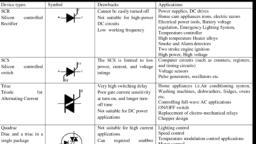
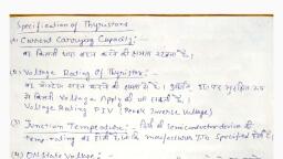
A silicon controlled rectifier or semiconductor-controlled rectifier is a four-layer, solidstate current-controlling device. The name "silicon controlled rectifier" is, General Electric's trade name for a type of thyristor., SCRs are mainly used in electronic devices that require control of high voltage and, power. This makes them applicable in medium and high AC power operations such, as motor control function., An SCR conducts when a gate pulse is applied to it, just like a diode. It has four layers, of semiconductors that form two structures namely; NPNP or PNPN. In addition, it, has three junctions labeled as J1, J2 and J3 and three terminals anode,cathode, , and a gate. An SCR is diagramatically represented as shown below., , The anode connects to the P-type, cathode to the N-type and the gate to the P-type, as shown below., , In an SCR, the intrinsic semiconductor is silicon to which the required dopants are, infused. However, doping a PNPN junction is dependent on the SCR application.
Page 3 :
Characteristics of Thyristor, Thyristors can either be forward biased or reverse biased. We will see how, it works in both states., , Thyristors in Forward Biased State, When anode is made positive, the PN junctions at the ends are forward, biased and center junction (NP) becomes reverse biased. It will stay in, blocked (OFF) mode (also known as Forward Blocking Stage) till the time, it is triggered by Gate current pulse or the applied voltage reaches the, forward breakover voltage., Triggering by Gate Current Pulse – When it is triggered by the gate, current pulse, it starts conducting and will act as a close switch. The, Thyristors remains in the ON-state, i.e. it remains in the latched state., Here the gate loses its control to turn off the device., Triggering by Forward Breakover Voltage – When a forward voltage, is applied, a leakage current starts to flow through the blocking (J2) in, the middle junction of Thyristors. When voltage exceeds the forward, break over voltage or critical limit, then J2 breaks down and it reaches to, the ON state., When the Gate current (Ig) is increased, it reduces the blocking area and, so the forward break over voltage is reduced. It will turn ON when a, , minimum current called latching current is maintained.When the gate
Page 4 :
current Ig=0 and anode current falls below a certain value called holding, current during the ON state, it again reaches to its forward blocking state, , Thyristors in Reverse Biased State, If the anode is negative with respect to cathode, i.e., with the application, of reverse voltage, both PN junctions at the end i.e. J1 and J3 become, reverse biased and the centre junction J2 becomes forward biased. Only a, small leakage current flows through it. This is the reverse voltage, blocking mode or OFF state of Thyristor., When the reverse voltage is increased further, then at a certain voltage,, avalanche breakdown of J1 and J2 occurs and it starts conducting in the, reverse direction. The maximum reverse voltage at which a thyristor, starts conducting is known as Reverse Breakdown Voltage., Two transister analogy, Two transistor analogy of SCR is a method of representing SCR in the form of two, transistor model. This represents SCR is the combination of PNP and NPN, transistor., SCR or thyristor is a three terminal semiconductor device which having P-N-P-N, structure. The basic operating principle of SCR can understand by two transistor, method of SCR., , As per figure you can see two transistors equivalent circuit of SCR. From the figure,, you can see the base of the transistor T1 is work as the collector of the transistor T2, and collector of the transistor T1 work as the base of the transistor T2., Now here we find the expression for anode current of SCR.
Page 5 :
As per transistor leakage current equation,, Collector current is expressed as,, , Where α is the current gain of transistor and Icbo is the leakage current of the, common base transistor., For transistor T1 emitter current = anode current Ia and collector current Ic = Ic1, , Where α1 is the current gain of transistor T1., Similarly, for transistor T2, , Where α2 is the current gain of transistor T2. And emitter current of transistor T2 =, cathode current Ik., Hereby figure, you can see anode current Ia is the sum of two collector current: Ic1, and Ic2., , By putting Ik = Ia + Ig, anode current Ia will be,
Page 6 :
Turn ON and Turn OFF operation of SCR, , In above fig we have applied to variable gate voltage to the SCR . In this circuit the, anode is positive with respect to cathode and when switch is pressed the gate, voltage is applied to the SCR and SCR will be triggered otherwise it will remains into, conducting state this is the turn ON operation of SCR ., We can turn off the SCR by decreasing the anode current below holding, current . or we have to apply the reverse voltage across the SCR , then the SCR will, be turn OFF SCR is a current controlled device ,because the gate current controls, the SCR . SCR can be act as opener close switch . The ON state voltage drop, across the SCR is very low the SCR handle thousands of amphers current . SCR is, a trigger device, di/dt and dv/dt protection circuits foe SCR
Page 7 :
Above fig shows the dv/dt and di/dt protection circuits for SCR here in fig (a) the, SCR can be protected from the excessive current by connecting the inductor L in, series with SCR since the SCR is solid state power device therefor by using the, inductor L we can protect the thyristor by variable current., , The dv/dt voltage protection circuit is shown in fig © . In this circuit also the, , SCR can be protected from excessive voltage. The AC line voltage is forwarded by, p-n-junction diode D towards the electrolytic capacitor C. therefore the charging and, discharging action of the capacitor while decide the operation of SCR this circuit is, also called as snubber circuit ., The SCR can be turn on or off by using snubber circuit . This circuit is widely, employed for most power system plants in electronic industry., TRIACThe acronym TRIAC stands for Triode for Alternating Current. A TRIAC is a, semiconductor device with three terminals that control the flow of current, thus the, name Triac. Unlike SCR, TRIAC is bi-directional while SCR is bi-directional. It is ideal, for operation utilizing AC power for switching purposes since it can control current
Page 8 :
flow for both halves in an alternating current cycle. This explained clearly in the, diagram below., , TRIAC Symbol, The circuit diagram for a TRIAC is shown below. It resembles two thyristors placed, back to back., , TRIAC Operation, The operation of the TRIAC is 7based on the thyristor. It facilitates the switching, function in AC electrical components and systems. They are widely used in light, dimmers because they allow both halves of the AC cycle to be utilized. As a result,, this makes them more efficient in power usage. As much as it is possible to use, thyristors to function as TRIAC, it is not cost efficient for operations that require low, power. It is possible to view a TRIAC in terms of two thyristors.
Page 9 :
TRIACs are normally used in applications that do not require very high power, because they exhibit non-symmetrical switching in their operation. This is, disadvantageous for applications utilizing high power as it causes electromagnetic, interference. As a result, TRIACs are used in motor controls, light residential light, dimmers and small electric fans to control speed., , TRIAC Basics, The triac is an important member of the thyristor family of devices. It is a bidirectional, device that can pass the current in both forward and reverse biased conditions and, hence it is an AC control device. The triac is equivalent to two back to back SCRs, connected with one gate terminal as shown in figure., TRIAC is an abbreviation for a TRIode AC switch. TRI means that the device, consisting of three terminals and AC means that it controls the AC power or it can, conduct in both directions of alternating current., , The triac has three terminals namely Main Terminal 1(MT1), Main Terminal 2 (MT2), and Gate (G) as shown in figure. If MT1 is forward biased with respect to MT2, then, the current flows from MT1 to MT2. Similarly, if the MT2 is forward biased with, respect to MT1, then the current flows from MT2 to MT1.
Page 10 :
The above two conditions are achieved whenever the gate is triggered with an, appropriate gate pulse. Similar to the SCR, triac is also turned by injecting, appropriate current pulses into the gate terminal. Once it is turned ON, it looses its, gate control over its conduction. So traic can be turned OFF by reducing the current, to zero through the main terminals., , It is possible to connect various combinations of negative and positive voltages to, the triac terminals because it is a bidirectional device. The four possible electrode, potential combinations which make the triac to operate four different operating, quadrants or modes are given as., , 1. MT2 is positive with respect to MT1 with a gate polarity positive with, respect to MT1., 2. MT2 is positive with respect to MT1 with a gate polarity negative with, respect to MT1., 3. MT2 is negative with respect to MT1 with a gate polarity negative, with respect to MT1., 4. MT2 is negative with respect to MT1 with a gate polarity positive with, respect to MT1., In general, latching current is higher in second quadrant or mode whilst gate trigger, current is higher in the fourth mode compared with other modes for any triac., Most of the applications, negative triggering current circuit is used that means 2 and, 3 quadrants are used for a reliable triggering in bidirectional control and also when, the gate sensitivity is critical. The gate sensitivity is highest with modes 1 and 4 are, generally employed., Advantages of TRIAC, •, , It is a bidirectional device , so we can control the power which is deliver to the, load in both half cycle of AC supply., , •, , It can design the TRIAC by using two SCR connected in anti parallel., , •, , We can operate the TRIAC by using positive and negative gate voltage ., MOS Controlled Thyristor, In above fig shows the vertically oriented structure of MOS controlled thyristor, this device has common characteristics like silicon controlled thyristor shows, the alternate combination of semiconductor layer having the positive and
Page 11 :
negative polarities for the formation of drift layer. The MOS controlled thyristor, is nothing but it is a combination of two MOSFET having p channel and n, channel facility., When we have to turn ON our MCT then we to apply positive gate voltage, to the gate terminals and during a turn OFF process or negative gate is MCT, , has low ON state voltage drop and turn ON time is about 0.4 msec. similarly, the turn OFF of time is 1.25msec . This power device can be operated up to, 500v with current rating 300ampere therefore is as very low switching loss, .This device also low reverse blocking capacity having maximum input, impedance . The MCT requires some time a simple driving circuit ,because for, maximum current the gate driving circuit is connected in parallel with MOS, controlled thyristor., , Fig. 4 – Voltage Ampere (VI) Characteristics of Thyristor
 Learn better on this topic